
Invented by Lee; Jeonghyeon, Jo; Minseok, Kang; Hyungkoo, Lee; Jonghan, SAMSUNG ELECTRONICS CO., LTD.
Integrated circuits are the tiny brains inside almost every electronic device. They keep getting smaller, faster, and more reliable. But as we keep shrinking them, new problems pop up. This blog post will help you understand one of the newest solutions: a clever way to arrange the parts on the “backside” of these chips so they work better and don’t make mistakes. We’ll break down what’s happening in the world of chips, why this invention matters, what came before, and what exactly is new here. Let’s get started.
Background and Market Context
Electronic devices are everywhere. From your phone and computer to your car and even your refrigerator, they all have integrated circuits (ICs) inside. These ICs are made up of tiny switches called transistors. Over time, chip makers have made these switches smaller and packed more of them into each chip. The more switches you have, the more powerful and useful your device can be.
But making chips smaller isn’t easy. When you pack parts closer together, you risk problems like short circuits, where electricity goes where it’s not supposed to. That can make devices fail or cause glitches. At the same time, people want their electronics to be fast, use less power, and not overheat. Chip companies are always looking for new ways to keep chips reliable, fast, and energy-efficient as they get smaller.
One of the biggest challenges is how to arrange the tiny wires and connections inside these chips. In the past, most of the connections and wires were placed on top of the chip. But as space runs out, engineers are now using the backside of the chip, too. This is called “Backside Power Delivery” or “Backside Contact Structure.” It’s a new way to add more wires and connections without making the chip bigger.
The market for these advanced chips is huge. Tech giants like Apple, Samsung, Intel, and TSMC are all racing to use these new methods. They want to make their chips smaller, faster, and cheaper. If you can make a chip that uses less energy, runs cooler, and fits in a smaller space, you have a big advantage. That’s why inventions like the one we’re talking about today are so important.
To sum up, the world needs better, smaller, and more reliable chips. The move to use the backside of chips for connections is one of the biggest trends in the industry right now. This patent application shows a new way to solve some of the toughest problems that come up when you try to do this.
Scientific Rationale and Prior Art
To really understand this invention, we need to talk about how chips are built and what problems engineers face.
Inside a chip, you’ll find layers of materials. Some carry electricity (conductors), some block it (insulators), and some do both depending on how you treat them (semiconductors). The transistors—the tiny switches—are made by stacking and shaping these materials in very precise ways.
In older chips, all the wiring was on the top. But as more transistors were squeezed in, there wasn’t enough space. That led to longer wires, which slowed things down and wasted energy. Imagine if your house had all the electrical wiring running through just one floor, even for the top rooms—it wouldn’t work very well. So, engineers started using the backside of the chip for some of the connections, especially for power and ground lines.
But using the backside isn’t as simple as flipping the chip over. You have to make tiny “vias” (vertical wires) that pass through the chip to reach the backside. These vias must be carefully placed and insulated, or else they might connect to the wrong part and cause a short circuit or leakage current—where electricity sneaks through places it shouldn’t. This can cause errors, heat, or even chip failure.
Before this invention, other engineers tried different ways to protect these vias. Some used extra layers of insulators. Some changed the shape or material of the vias. Others made wider spaces between wires, but that eats up valuable chip space.
Another big step in chip design was the “Gate-All-Around” (GAA) transistor. This design wraps the control gate all the way around the channel where electricity flows, making it easier to control and less likely to make mistakes. But GAA designs are even more sensitive to layout problems, especially when you start connecting power from the backside.
Prior solutions often had trade-offs. They might work, but only if you made the chip bigger, or they were hard to manufacture, or they didn’t fully stop leakage currents. Some designs used extra thick insulation, but that slowed down signals or made the chip too tall. Others could leak during manufacturing, damaging sensitive areas inside the chip.
In summary, the key problems are: how do you add backside connections without causing shorts or leakage, and how do you keep the chip small and fast? Past solutions didn’t get it quite right. That’s where this new invention comes in.
Invention Description and Key Innovations
This invention tackles the problem of making backside connections in a chip that is both tiny and packed with advanced GAA transistors. The goal is to allow lots of connections in a small area, keep everything insulated, and avoid any unwanted current leaks or short circuits.
Let’s walk through the main features in simple terms:
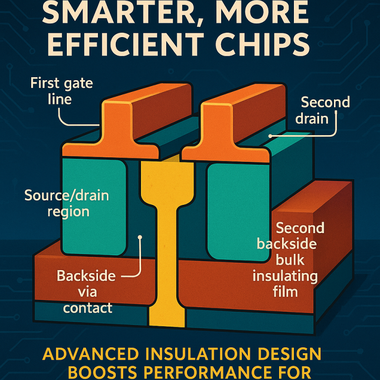
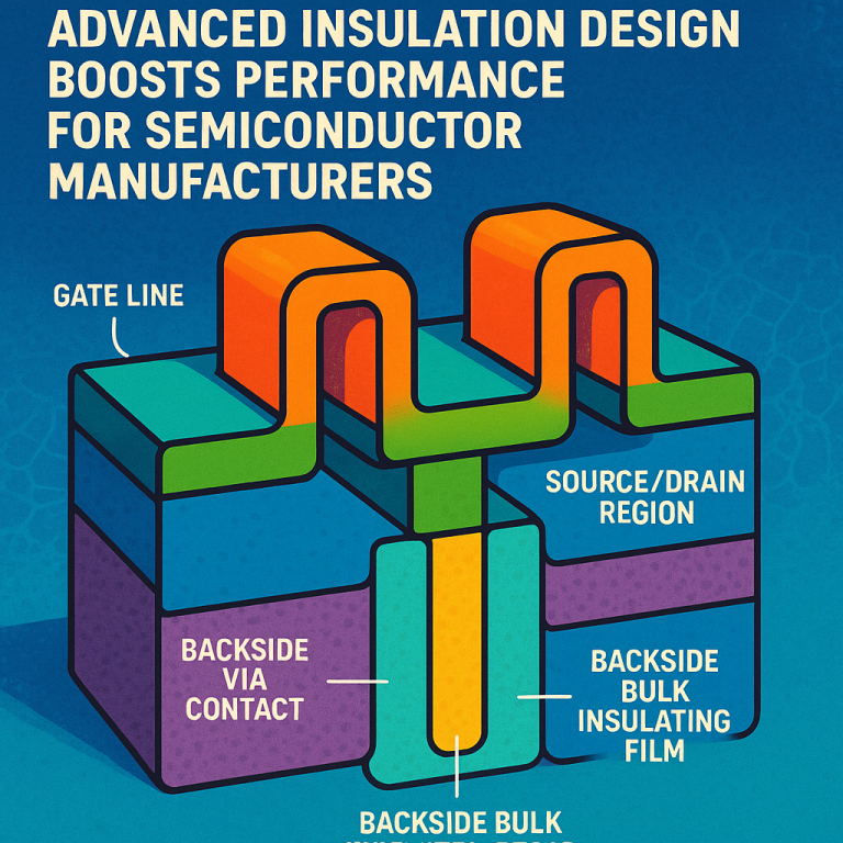
The chip has two main types of lines next to each other: gate lines (which control the transistors) and power lines (which bring electricity in and out). Between the gate lines, you have a region called the source/drain. This is where current enters and leaves each transistor.
To connect this source/drain region to the backside of the chip, the design uses a “backside via contact.” Think of this as a tiny metal rod that goes straight down from the source/drain, through the chip, to the bottom. This rod must be carefully insulated so it doesn’t touch anything else by accident.
What’s new here is how the insulation is set up. Instead of just wrapping the via in a single layer, the design uses a “backside bulk insulating film” made out of special materials like silicon nitride (SiN), silicon carbonitride (SiCN), or similar. This film has a unique shape: it has both vertical and horizontal parts.
The vertical part sits right under a gate line and stretches down. The horizontal part sticks out from the side of the vertical part, reaching over to touch the source/drain region. The via contact is placed carefully between two of these insulating films. In other words, the via is sandwiched between two strong barriers, each made of both vertical and horizontal insulation.
Each part of the insulation does a job. The vertical piece keeps the via from getting too close to the gate lines. The horizontal piece blocks any sideways current that might sneak from the via to the source/drain or other regions. By combining these shapes, the design traps the via in a “box” of insulation. This stops unwanted currents and makes the whole chip more reliable, even as it gets smaller.
There are other clever touches, too. The insulating films can be made of different materials to match the needs of each area. They can also be stacked, shaped, or even combined with other insulators if needed. The design also includes “nanosheet stacks” for the GAA transistors, with the insulation carefully arranged so that every part of the transistor is protected but still easy to connect.
The invention also describes how these parts can be made in a real factory. It explains which layers to build first, which to etch or remove, and how to line everything up so the vias and insulation end up in just the right place. It even includes ways to make sure the sensitive gate dielectric (the layer that controls the transistor) isn’t damaged during all these steps.
By doing all this, the invention makes it possible to put lots of backside connections in a tiny space, keep them safe from shorts or leaks, and still use the newest, fastest transistor designs. This means faster, smaller, and more reliable chips for everything from phones to servers to self-driving cars.
What Makes This Invention Stand Out?
The real breakthrough is the way the insulation is shaped and placed. Instead of just adding more material or more space, the design uses vertical and horizontal parts that work together. This clever geometry keeps every connection safe while using as little space as possible.
The invention also lets chipmakers use different materials or thicknesses for different parts of the chip. This means you can fine-tune the insulation for each area, getting just the right balance between protection and speed.
Finally, the patent explains exactly how to build these chips using common manufacturing steps. That means it can be used in real factories, not just in theory.
How Does This Help?
With this design, chipmakers can make chips that are smaller, use less energy, and are less likely to fail. Devices can be faster and last longer on a battery. New features, like AI or super-fast graphics, can fit in smaller gadgets. And since the process works with the latest types of transistors, it’s ready for the future.
Looking Ahead
As chips keep shrinking, solutions like this one will only become more important. The clever use of insulation, the careful shapes, and the smart manufacturing steps all point toward a future where chips are both tiny and tough. Whether you’re a chip designer, a tech company, or just someone who loves gadgets, this kind of invention is what keeps the digital world moving forward.
Conclusion
Chips are the heart of modern devices, but making them smaller and better is a huge challenge. This new patent shows a smart way to connect the backside of a chip while keeping everything safe and reliable. By using special-shaped insulating films, clever layouts, and proven materials, this invention solves real problems facing chipmakers today.
If you’re working in chip design, manufacturing, or even just following tech trends, this is an important step. It means better, faster, and more reliable devices for everyone. As the world keeps asking more from our electronics, inventions like this will keep us moving forward.
Stay tuned for more updates on chip technology and what they mean for the devices you use every day. If you want to learn more, reach out to our team of patent experts at Inventiv—we’re here to help you understand and protect the next big idea.
Click here https://ppubs.uspto.gov/pubwebapp/ and search 20250366013.