Invented by SHIN; Hyun Eok, PARK; Joon Yong, SO; Byung Soo, YANG; Su Kyoung, LEE; Dong Min, JANG; Keun Ho
This article breaks down a recent patent application for a new kind of display device. We’ll look at why these displays matter, the science and older inventions behind them, and what’s new and special in this one. By the end, you’ll have a plain-English guide to how the device works and why it’s important.
Background and Market Context
Displays are everywhere. From phones to TVs, from smartwatches to car dashboards, displays bring information to our eyes. Over the years, people have wanted screens that are brighter, thinner, longer lasting, and less likely to break. At the same time, companies want to make displays that use less power and last longer. Every day, scientists and engineers hunt for better ways to build these screens.
The market for display devices is huge. Billions of people use devices with screens daily. Companies compete to make the best displays because better displays can mean more sales. For example, a phone with a screen that looks great in sunlight or lasts longer on one charge has a big advantage. So there is a lot of money and effort spent on making displays better, cheaper, and more reliable.
But making a great display is not easy. Light-emitting elements (the tiny parts that make the screen glow) can be damaged by things like water in the air. If even a tiny bit of moisture gets inside the screen, it can cause problems. Also, the layers inside a display must stick together very well. If they don’t, the layers might peel apart, and the screen can stop working. This is called “delamination” and it’s a big worry for anyone making displays.
Today’s market also expects displays to be flexible sometimes, or to fit into odd shapes. That means new materials and new ways of putting the layers together. Every new phone, smartwatch, or tablet pushes for thinner, lighter, and more durable displays. As a result, patents like this one are important because they promise a way to address the problems of sealing out water, keeping the layers together, and making electrical paths more stable.
In short, the background to this patent is a market that wants better screens—brighter, longer lasting, and tougher. This patent claims to offer a way to make these improvements real.
Scientific Rationale and Prior Art
Let’s talk about the science behind these displays and what has been done before. Modern displays often use something called OLEDs—organic light-emitting diodes. These are small parts that glow when electricity runs through them. Each screen has many pixels, and each pixel may have red, green, and blue sub-pixels to make all the colors you see.
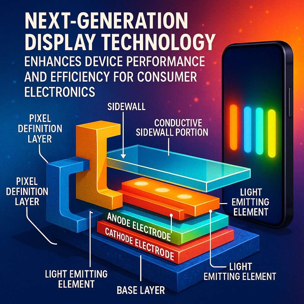
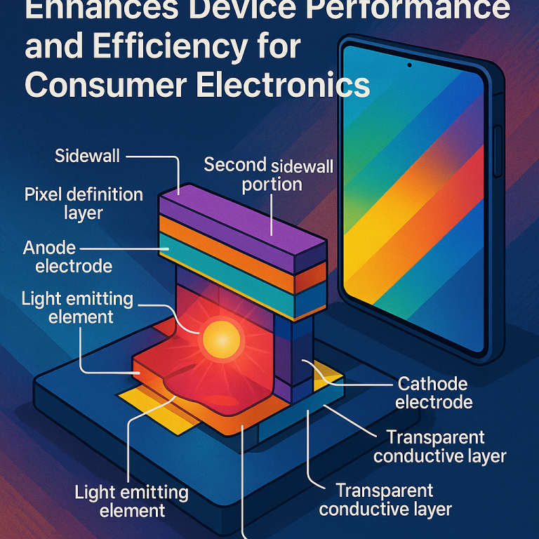
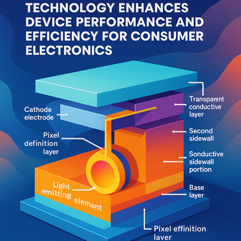
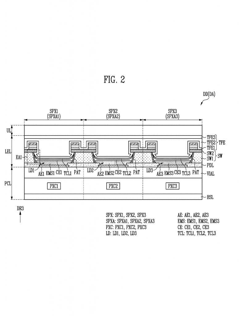
Each of these tiny light-emitting parts is built in layers. At the bottom, you usually have a base layer, which can be glass or plastic. On top of that, you add electrodes—these are the anode and the cathode, which let the electricity flow. In between, there is an emission structure, which is the real “engine” that lights up.
To keep the light from spreading everywhere, and to make sure each color only shows where it should, you need special layers. One of these is called the pixel definition layer. It helps keep the light in the right spot. Around the edge of each pixel, you might see sidewalls—these help with structure and keeping the layers where they belong.
A big problem in older displays was that the layers sometimes lifted up or peeled off from each other. This could let water or air slip inside, which could damage the sensitive parts. To stop this, companies tried to make the layers stick together better. They also tried to make sure the electrical paths—the ways electricity moves through the screen—stayed stable, even as the screen got hot or cold or was bent.
In the past, companies used things like aluminum or silver for the electrodes because they are good at conducting electricity. Sometimes, they used transparent conductors (like indium tin oxide) so that light could get out through the top layer. People also tried to use different materials for the sidewalls, hoping to get the best mix of strength and conductivity.
Some tried putting extra coatings on the sidewalls to help the layers stick. Others changed the way the layers were deposited—using sputtering (a way of “spraying” thin layers of metal or oxide) instead of older techniques like thermal evaporation. Each change was meant to fix problems like peeling, water getting in, or unstable electrical connections.
Despite all this work, problems remained. Sometimes the cathode (the negative side of the electrical circuit) did not stick well to the sidewall, especially if there was a thin layer of oxide on the surface. This could mean higher electrical resistance or even a broken connection. If the layers did not fit closely, water could sneak in, and the screen would fail. Also, some older ways of making the layers required many masks (like stencils) and extra steps, which made manufacturing slow and expensive.
So, the scientific rationale for this new invention is to solve these old problems: make the layers stick better, keep water out, and ensure the electrical paths are stable and reliable, while also making the device easier and cheaper to build.
Invention Description and Key Innovations
Now let’s look at what’s actually new and special in this patent. The invention describes a display device made up of several carefully arranged layers and structures, each chosen and designed to address the problems we covered before.
At the heart of the invention is a new way to build up the layers, especially around the sidewalls and the connections between the parts that carry electricity. Here’s how the new display is made and why it matters.
First, the base layer acts as the foundation for the display. On this base, the anode electrode is placed. This electrode is where positive charge enters the light-emitting element. Part of the anode is covered by a pixel definition layer, but some of it is left exposed, which is important for making good electrical connections later.
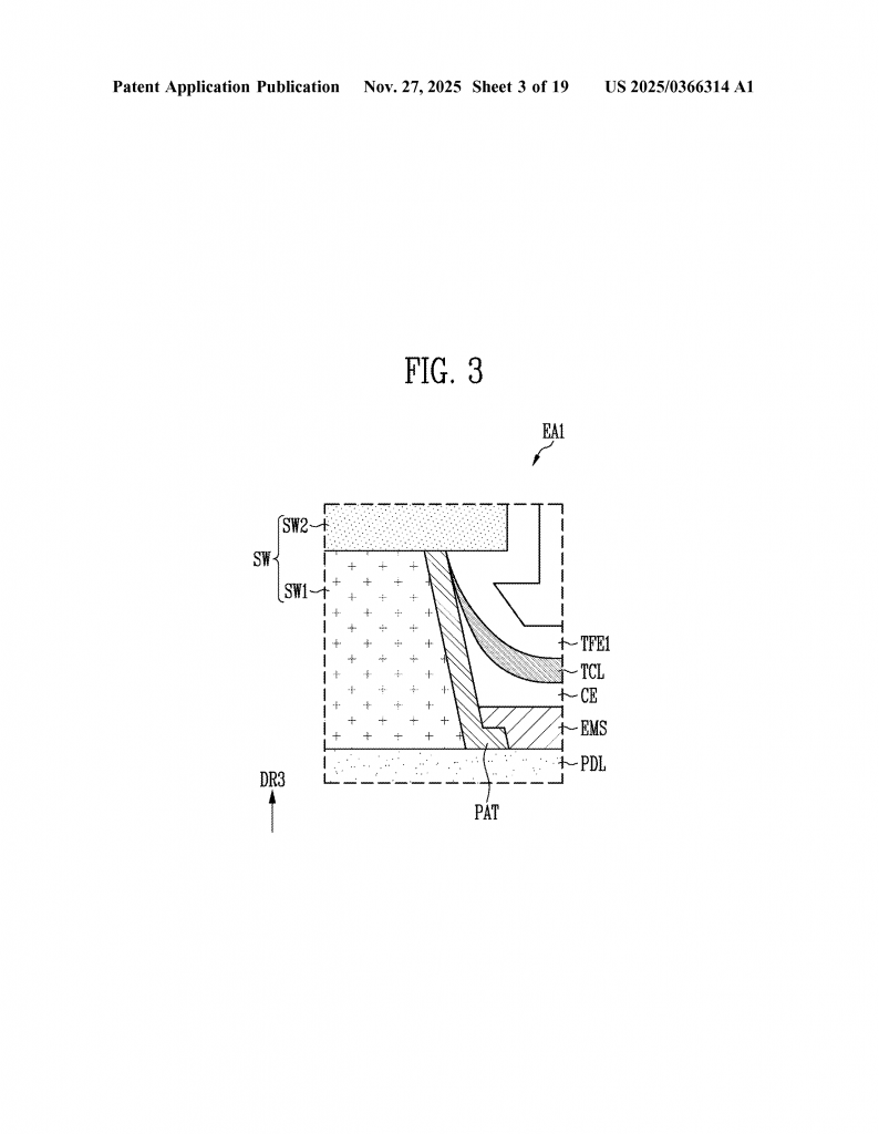
On top of the pixel definition layer, the display adds a sidewall. This sidewall is actually made in two pieces: a first sidewall and a second sidewall on top. The first sidewall is often made from aluminum, which is very good at carrying electricity. The second sidewall, sitting on the first, is made from titanium. Titanium is not as good at conducting electricity, but it is tougher in the face of certain manufacturing steps, like etching (where parts of a layer are removed to create the right shapes).
The real innovation comes with the “conductive sidewall portion.” This is a thin layer, usually made from titanium, titanium nitride, or molybdenum, that wraps around the side of the first sidewall. This layer is carefully patterned so that it covers the side surface of the first sidewall, and sometimes covers part of the anode as well.
Why is this important? When you make the first sidewall out of aluminum, it can form a thin layer of aluminum oxide on its surface—especially when exposed to air. This oxide makes it hard for the next layers to stick well, which can lead to weak spots or poor electrical contact. By adding a thin, well-chosen conductive layer on top, the invention ensures that the cathode electrode (the next layer that goes on top) sticks well and carries electricity efficiently. This reduces the chance of the layers peeling apart and makes the screen more reliable.
The way these layers are built is also clever. The process uses sputtering (a way of spraying on thin films of material) instead of older methods. Sputtering lets the conductive sidewall portion wrap fully around the side of the first sidewall, even if that side is angled or has a tricky shape. After sputtering, the extra material is etched away using a special type of etching (anisotropic dry etching), so that only the part under the second sidewall remains. This means the layers can be shaped exactly as needed without extra masks or steps.
On top of the emission structure (the part that actually glows), a cathode electrode is placed. This electrode is usually silver, which is a very good conductor. The cathode may fully or partly cover the conductive sidewall portion, depending on the exact design. It is carefully connected to the first sidewall through the conductive sidewall portion, making sure the electrical path is solid and reliable.
The entire stack is then topped with a transparent conductive layer, made from materials like indium tin oxide or similar compounds. This layer lets light escape from the screen while still carrying electrical current. By fully covering the cathode and the conductive sidewall, this layer adds another level of protection and helps the next layer (the encapsulation layer) stick well. The encapsulation layer then seals everything, keeping out moisture and dust.
In some cases, the process of building the display is changed a little. For example, sometimes the pixel definition layer is patterned first, and the anode is exposed. Other times, the pixel definition layer is put down first, then the conductive sidewall portion is added, and only then is the anode exposed. This allows for even greater control and can reduce the chance of damaging the anode during manufacturing.
The invention also covers displays with sub-pixels for different colors—red, green, and blue—each built in its own area with its own anode, emission structure, and cathode. The same layering system applies to each color, making the whole display work better.
Finally, the patent describes how this display can be used in all sorts of electronic devices—not just phones and tablets, but watches, laptops, even car screens and head-mounted displays. The method for making the display is also covered, so manufacturers can use the techniques to build better screens across many products.
In summary, the key innovations are:
- A special, thin conductive sidewall portion that helps the cathode stick and carry electricity.
- Careful choice of materials (aluminum, titanium, silver, ITO, etc.) for each layer.
- A new way of layering and etching that simplifies manufacturing and improves reliability.
- Better sealing against moisture and stronger adhesion between layers, reducing the risk of peeling or failure.
- Flexible design that works for many kinds of displays and devices.
Conclusion
This new patent offers a smart approach to one of the toughest problems in display technology: keeping all the layers close together, ensuring reliable electrical paths, and sealing out things like water that can ruin a screen. By using a clever mix of materials and new ways to build each layer, the invention promises displays that last longer, work more reliably, and can be made more easily. For anyone interested in how the screens in our devices work—and how they might get better in the future—this patent is a great example of progress in making everyday technology more robust and user-friendly.
Click here https://ppubs.uspto.gov/pubwebapp/ and search 20250366314.