Invented by ZHUANG; Li, KITSOMBOONLOHA; Rungrot
Liquid crystal displays (LCDs) are all around us—from our phones to TVs, and now, even in headsets and smart glasses. But, did you know that inside every tiny display, there are even tinier structures called spacers that make a huge difference in how clear and reliable your screen is? In this article, we’ll break down a new patent application for a special LCD cell design, especially for near-eye displays like VR headsets and AR glasses. We’ll look at why the market needs this, the science behind it, and what makes this invention stand out.
Background and Market Context
The world is moving fast towards devices that bring digital images closer to our eyes than ever before. Think about virtual reality (VR) headsets, augmented reality (AR) glasses, and mixed reality (MR) systems. These gadgets need screens that are not only bright and sharp but also small and light enough to wear on your face for hours. That’s where near-eye displays come in.
A near-eye display puts a screen just a few millimeters in front of your eyes. Because the display is so close, even tiny problems—like a small dark spot or a blurry area—can ruin the whole experience. The eyes are extremely sensitive to changes in brightness, color, and clarity, especially when the display fills your entire field of view.
Users expect these devices to give them realistic, immersive images with no distractions. But making screens this small and this clear is not easy. As companies push for higher resolution and smaller pixels, they face new challenges. One of the biggest problems is keeping the display uniform—making sure every part of the screen looks the same, with no funny spots or lines.
LCDs work by controlling light as it passes through a thin layer of liquid crystal, sandwiched between two pieces of glass or plastic. To keep the two sides from touching each other, tiny spacers are placed between them. If these spacers move or get out of place—even by a tiny amount—they can cause marks or “blemishes” on the screen, called “mura.” In Japanese, “mura” means “blemish” or “unevenness.” For near-eye displays, even the smallest mura is a big problem.
As the market for VR, AR, and MR devices grows, so does the need for better, more reliable near-eye displays. Users want bigger fields of view, crisper images, and lighter devices. This puts pressure on display makers to shrink every part of the screen, including the spacers. But as spacers get smaller, they get harder to keep in place. This leads to more mura problems, especially when the display is bent, pressed, or dropped.
The new invention described in this patent application is all about solving these problems. It introduces a clever way to design the spacers, so they stay put and keep the display uniform and clear, even as the screens get smaller and more advanced.
Scientific Rationale and Prior Art
To really understand what’s new here, let’s look at how LCDs have worked up until now, and why traditional solutions fall short for near-eye displays.
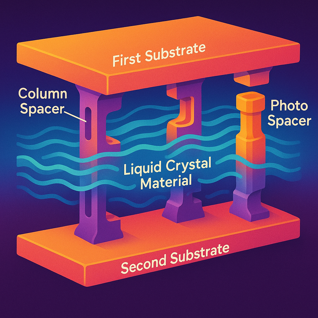
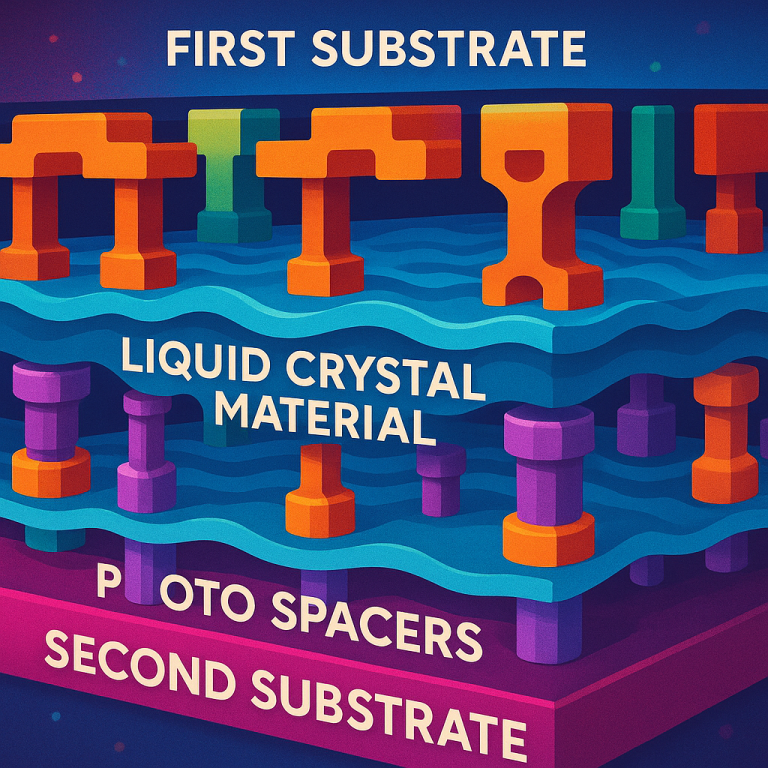
A typical LCD panel is made of two flat layers (usually glass). Between them is a thin layer of liquid crystal. When an electric signal is applied, the liquid crystal changes how light passes through, creating images. To stop the two layers from touching each other, small “spacers” are used. These are like tiny pegs or posts, sprinkled across the display. There are two main kinds:
Column spacers are usually made on the lower glass and are shaped like small columns.
Photo spacers are formed on the upper glass, made by shining light through a mask to harden certain areas of a special material.
When the two sides are put together, the photo spacers rest on top of the column spacers. This keeps the gap between the layers even, which is important for the display to work properly.

But in high-resolution LCDs, the pixels (the tiny dots that make up the screen) are very small. This means the spacers also have to be small, often less than 10 micrometers wide (about 1/10th the width of a human hair). If the display is bent, pressed, or shaken, these small spacers can slip out of place, causing the layers to touch where they shouldn’t. This can create dark or bright spots, lines, or other marks on the display—what we call “mura.”
Previous designs tried to solve this problem by making the spacers bigger or adding more of them. But bigger spacers block light and lower image quality. Adding more spacers takes up space that could be used for pixels, making the display less sharp. Other designs used sticky materials or different shapes, but these often made the manufacturing process more complicated or didn’t fully solve the issue.
Some advanced designs used special shapes, like tapered or rounded spacers, to help keep them in place. Others tried putting spacers at different heights or in different patterns. But as the industry moves toward higher resolutions and thinner screens, even these solutions are not enough. The risk of mura remains, especially in devices that are handled a lot, like VR headsets or AR glasses.
So, the need is clear: a new way to design spacers that keeps them in the right place, allows the display to move a little without causing damage, and doesn’t block light or make the screen less sharp. That’s where the new invention stands out.
Invention Description and Key Innovations
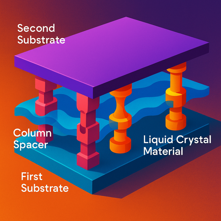
Now, let’s dig into what’s really new and special about this patent application. The invention introduces a clever way to design the spacers in LCD cells—especially for near-eye displays—so they stay in the right place even when the display is bent or pressed.
Instead of using plain, single-piece spacers, this design splits either the column spacers or the photo spacers (or both) into two parts. These two parts are arranged to form a small “recess” or “pocket” between them. The matching spacer from the other substrate (the other side of the screen) fits into this pocket, almost like a puzzle piece. This design keeps the spacers locked together, making it much harder for them to slip out of place.
For example, imagine the column spacer is split into two pieces, with a gap between them. The photo spacer on the other side is shaped to fit right into that gap. If the display is pushed or bent, the photo spacer can move a little inside the pocket, but it can’t slide away and touch the wrong part of the display. Even if the layers move sideways a bit, the spacers remain engaged, keeping the gap between the layers safe and uniform.
The sides of the pocket can be rounded or slanted outward, making it easier for the matching spacer to fit in, and allowing just enough movement to absorb any small bumps or pressure. The shape of the spacers can be round, oval, rectangle, or parallelogram, depending on the design needs.
This “split and pocket” design can be done in either direction:
– The column spacer (on the bottom layer) can be split, with the photo spacer (on the top layer) fitting into the pocket.
– Or, the photo spacer can be split, with the column spacer fitting into the pocket.
The patent also describes arranging these split spacers in different patterns across the display. For example, some pockets can be slanted in different directions (like northeast or northwest) so that movement in any direction is limited. This makes the whole display more stable and less likely to develop mura, no matter how it’s handled.
Another smart idea is using spacers of different heights and types. Some spacers act as the main support, setting the gap between the layers. Others are “safeguard” spacers—they’re a bit taller or shorter and are placed near the main spacers. If there’s a big movement, the safeguard spacers catch the layers and stop them from crashing into each other, preventing damage.
The design can use a mix of spacer shapes and patterns, giving engineers a lot of flexibility. For example, round spacers can be used where light must pass through, while slanted or parallelogram spacers can be placed where extra support is needed.
Key benefits of this invention include:
– Better control of layer movement, making the display more durable.
– Less risk of mura, even in high-resolution and thin displays.
– Flexible design options for different screen sizes and shapes.
– No need to make spacers bigger, so image quality stays high.
– Simple changes to the manufacturing process, so it can be used with existing LCD lines.
This design is especially helpful for near-eye displays, where the screen is close to the eye and small defects are easy to see. By keeping the spacers in the right place, even as the industry pushes for smaller, lighter, and sharper screens, this invention helps deliver the kind of clear and uniform images that users expect from the next generation of VR, AR, and MR devices.
Conclusion
As we move into a world where screens are closer to our eyes and higher in resolution, the smallest details matter more than ever. This patent application presents a smart and practical way to keep LCD spacers exactly where they should be. By splitting spacers and creating interlocking pockets, the design holds the screen layers steady and stops defects before they start. For device makers, this means more reliable products. For users, it means clearer, more immersive experiences. As VR, AR, and MR devices become part of everyday life, innovations like this will make all the difference.
Click here https://ppubs.uspto.gov/pubwebapp/ and search 20250334837.