Invented by PARK; Youngseok, YOON; Hyunchul, IHM; Jeongdon, KANG; Yeongwoo, KIM; Yongjun, PARK; Keonwoo, PARK; Chulkwon, LEE; Changyoung, JUNG; Sanghoon, Samsung Electronics Co., Ltd.
Memory chips are the heart of every electronic device, from your phone to high-end servers. As gadgets get smaller and smarter, memory needs to work faster and fit into tinier spaces. Today, we’ll explore a new patent that promises to change how memory chips are built and how they perform.
Background and Market Context
For decades, companies have pushed to make computers, phones, and other gadgets smaller, faster, and more powerful. Much of this progress has come from making memory chips—especially DRAM (Dynamic Random Access Memory)—smaller and able to hold more data. DRAM is the fast, temporary memory every modern device uses to keep things running smoothly. It’s what makes your apps open quickly and your games run without lag.
But shrinking DRAM and other memory chips isn’t easy. As the parts inside these chips get tinier, it becomes harder to squeeze in all the circuits needed to make them work. Memory chips are made of millions (even billions) of tiny cells, each storing a bit of information. These cells are laid out in a big grid, called an array. To read or write data, special circuits need to turn on and off the right rows and columns inside this array.
Most memory chips today use something called a “cell on periphery” (CoP) structure. This means that the main logic circuits that control the memory are placed under the memory cells themselves. This design helps save space, but it creates new challenges. The circuits that sense and move data (like sense amplifiers and wordline drivers) must be arranged very carefully so the chip works quickly and reliably.
The market is hungry for new ideas that can make memory chips smaller, cheaper, and faster. Phones, laptops, game consoles, and big data centers all need better memory. At the same time, there’s a push for “vertical” designs, where memory cells stack upward, not just across a flat chip. This helps pack more memory into a small space, but it also makes designing and connecting all the control circuits much harder.
This patent comes at a time when the need for high-capacity, fast, and efficient memory is greater than ever. If you can make memory chips with better layouts, you can build smaller gadgets, longer-lasting phones, and more powerful servers. The ideas in this patent aim to solve key problems that have held back memory chip design for years.
Scientific Rationale and Prior Art
To understand why this patent matters, let’s look at how memory chips have been built until now, and what challenges they face.
In most DRAM chips, the memory cells sit in a grid, and special wires called wordlines and bitlines connect to each cell. Wordlines run across the rows, and bitlines run down the columns. When you want to read or write data, circuits called wordline drivers turn on a row, and sense amplifiers read the small signals on the columns.
Traditionally, DRAM used an “open bitline” structure. In this setup, each sense amplifier connects to a pair of bitlines—one for the signal, one for its opposite (complementary signal). This helps the sense amplifier tell the difference between a “1” and a “0” more easily. However, as chips have shrunk, this structure started to hit physical limits.
As cell sizes dropped and more cells were packed in, the wires connecting everything got longer and thinner. This made it harder for sense amplifiers to pick up signals quickly, which slowed down the chip and made it use more power. Also, the circuits that drive the wordlines and sense the bitlines took up a lot of space. Fitting all these circuits into the shrinking chip area without causing errors became a major challenge.
Another problem is that as memory cell transistors get smaller, their performance gets worse. Many companies are now using vertical channel transistors (VCTs), which stand upright instead of lying flat. This allows more cells in the same area, but makes it even trickier to place all the needed control circuits in a way that doesn’t slow down the chip or introduce errors.
Previous designs either spread the control circuits around the edge of the memory cell array, which wasted space, or tried to pack them under the cells, which caused problems with connecting everything together. Some tried to split the sense amplifiers and wordline drivers between different areas, but this often led to longer wires and slower performance.
What was missing was a smart way to split and arrange the sense amplifiers and wordline drivers under the memory cell array in a way that is both space-efficient and keeps the chip fast and reliable. This patent introduces a new layout that directly addresses these pain points.
Invention Description and Key Innovations
The heart of this patent is a new way to build the memory core circuit of a chip. Let’s break down what makes it different and why it matters.
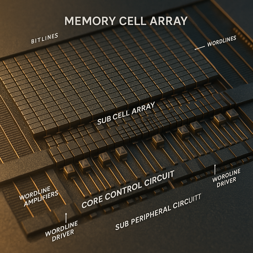
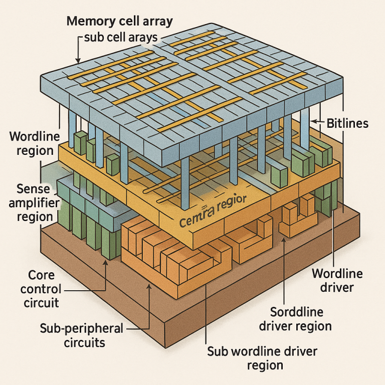
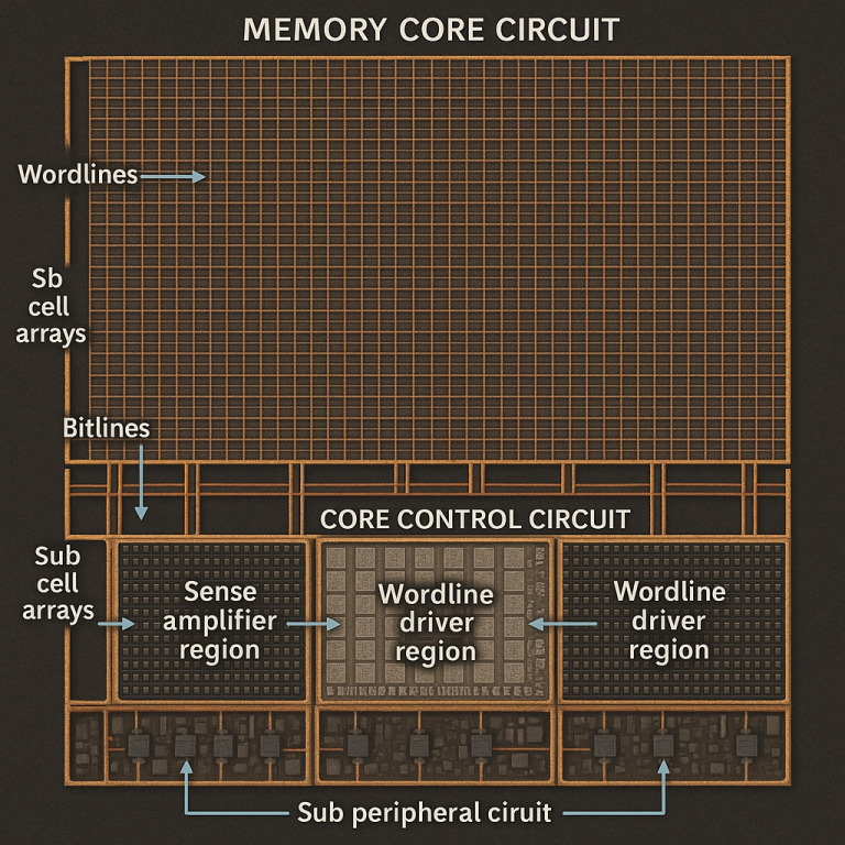
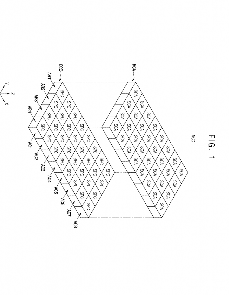
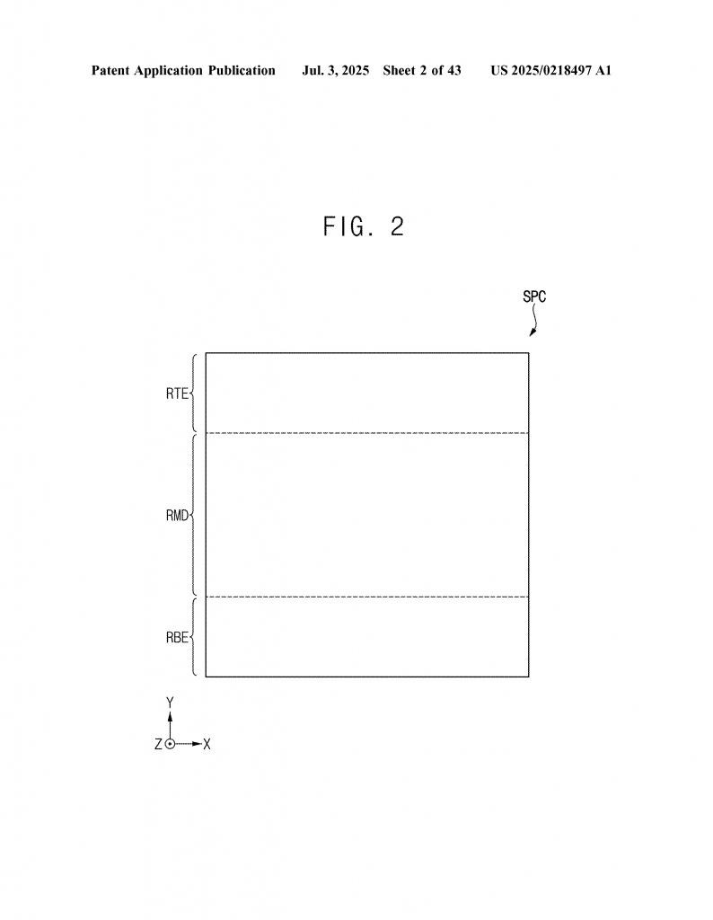
Imagine the memory cell array as a big grid, with smaller blocks called “sub cell arrays” arranged in rows and columns. Beneath each sub cell array, there is a “sub peripheral circuit.” These circuits are split into three regions:
– First column edge region (on one side)
– Second column edge region (on the other side)
– Central region (in the middle)
The sense amplifiers, which detect tiny signals from the memory cells, are placed at the edges—either in the first or second column edge regions, or both. This is smart because it puts the amplifiers close to the bitlines they need to sense, making their job easier and faster.
The wordline drivers, which turn on the rows of memory cells, are placed in the central region. This is important because it shortens the path between the driver and the wordlines, which helps the chip operate more quickly and reliably.
But the real genius is in how these regions are arranged. The central region can be split into two subregions, allowing for different layouts. For example, in some designs, one subregion holds the wordline drivers, while the other holds other circuits (the “rest region”). This allows flexibility in fitting in extra control circuits as needed.
The patent describes both “shift” and “mirror” structures. In a shift structure, the rest circuit region of one sub peripheral circuit is next to the wordline driver region of its neighbor. In a mirror structure, similar regions (like wordline drivers or rest circuits) are next to each other. These patterns help designers arrange the circuits in the most efficient way for their chip’s needs.
Another key idea is how the sense amplifiers are distributed. You don’t need every sub peripheral circuit to have the same number of amplifiers. In some designs, only the circuits on even columns have amplifiers, and the odd ones don’t. This reduces the total number of amplifiers needed, saving space and power. The bitlines are cleverly connected so that each amplifier can handle signals from both its own and neighboring sub cell arrays.
The chip can also use either a “closed” or “open” bitline structure, depending on what’s best for the application. In the open structure, each sense amplifier is connected to a bitline and a complementary bitline from an adjacent array, which improves efficiency and makes the chip easier to shrink further.
Another important feature is the use of vertical channel transistors in each memory cell, with the memory unit (like a tiny capacitor) stacked on top. This vertical design helps fit more memory into the same chip area, boosting capacity without needing more space.
To sum up, the main innovations in this patent are:
1. Dividing the control circuits under each sub cell array into three parts: sense amplifiers at the edges, wordline drivers in the middle, and other circuits where needed.
2. Flexible arrangements (shift or mirror) to suit different chip layouts and needs.
3. Smart distribution of sense amplifiers (not every block needs the same number), saving space and power.
4. Efficient connection of wordlines and bitlines to keep signal paths short and fast.
5. Support for both open and closed bitline structures for design flexibility.
6. Use of vertical transistors to make the most of chip area.
These changes add up to a memory chip that’s smaller, faster, and easier to design, with more room for extra features. It also makes it easier to scale up to bigger memory sizes, which is key for the next generation of devices.
Conclusion
The patented memory core circuit represents a big step forward for memory design. By cleverly arranging sense amplifiers and wordline drivers under the memory cell array, and offering flexible ways to connect and distribute these circuits, this invention tackles some of the toughest problems in modern memory chips.
For everyday users, this means smaller, faster, and more reliable devices. For chip designers, it opens new doors for building high-density memory chips that are easier to scale and adapt. As the demand for better memory continues to grow in everything from smartphones to servers, innovations like this will shape the future of electronics for years to come.
Click here https://ppubs.uspto.gov/pubwebapp/ and search 20250218497.