Invented by NGUYEN; Vanluan, KIM; Jaewon, KIM; Taehoon, SHIN; Hyeonjin, CHOI; Taejin, Samsung Electronics Co., Ltd.


Let’s talk about a new idea that could change the future of electronic devices. At its heart, the invention is about making a “stacked structure” that keeps its ability to insulate (called a low dielectric constant) even when it gets thicker. This is very important for electronic gadgets, big computers, and even your phone. We’ll walk through why this matters, what science and older ideas led to it, and then explain how this new invention works in the simplest way possible.
Background and Market Context
All our favorite devices—phones, tablets, TVs, and computers—are powered by tiny chips. These chips are packed with millions, sometimes billions, of even tinier circuits. To make these chips work fast and not overheat, engineers need to keep the metal wires inside them close together, but not too close. If they are too close, electricity can “jump” between them, causing problems. This “jump” is called parasitic capacitance. It slows things down and can make the device less reliable. The solution is to use a special kind of material between the wires called a “dielectric.” The lower its dielectric constant, the better it stops electricity from leaking between wires.
As companies try to make chips smaller and faster, the problem gets worse. Wires are closer together than ever before. If you use the wrong material, signals will get mixed up and the device won’t work well. The market for better dielectric materials is huge. Every phone, computer, camera, and smart watch depends on it. If someone finds a way to make a thicker, low-dielectric layer that works well, it can help make smaller, faster, and cheaper devices. Companies all over the world, from chip makers to display manufacturers, are searching for such solutions.
In the past, engineers used materials like silicon dioxide and silicon nitride as insulators between wires. These worked fine for a while, but as chips got smaller, they weren’t good enough. Newer materials like boron nitride and other compounds were tried because they have a lower dielectric constant. But there was a big problem: when you tried to make these layers thicker, they would stop working as well. They would turn from an “amorphous” (messy and disordered) state to a “crystalline” (ordered) state, and that made their dielectric constant go up. That’s bad news for chip makers.
The real market need is clear: find a way to make thick layers that keep their low-dielectric property. If you can do that, you help all kinds of devices run faster, use less energy, and stay cooler. This invention aims to solve exactly that challenge.
Scientific Rationale and Prior Art

Let’s look at how science explains this problem. When you want to keep electricity from leaking between wires, you need a material with a low dielectric constant. “Dielectric constant” is just a fancy way of saying how good the material is at not letting electricity pass through. The lower the number, the better it is at blocking electricity.
Materials like silicon dioxide (glass) and silicon nitride have been used for years. They are good but not great; their dielectric constants are not low enough for the newest, tiniest chips. So, scientists tried things like boron nitride and other “amorphous” materials. Amorphous means the atoms inside are jumbled up and not in a neat pattern. This jumbled-up state helps the material stay a good insulator.
But here’s the catch: When you make the layer thicker, it wants to change. The atoms start lining up into a crystal pattern. Once this happens, the dielectric constant goes up and it stops being a great insulator. In other words, making it thick ruins the very thing you wanted.
There have been some workarounds. One way was to keep the layer thin, but that often isn’t enough for real chips. Another was to try different materials, but none really solved the problem. Some tried putting a thin “barrier” layer between the insulating layers, hoping it would stop the atoms from rearranging. Sometimes it worked, sometimes it didn’t.
Other people have used two-dimensional materials like graphene or molybdenum disulfide as barriers, but usually just as a single layer in a device, not as a repeating stack. The problem with these earlier ideas is that they either didn’t keep the dielectric constant low enough when the stack got thicker, or they made the process too complex for real factories.
So, to sum up: Science says thick amorphous layers want to turn into crystals when they get too thick, and that makes them bad insulators. Earlier ideas tried thinner layers, different materials, or simple barrier layers, but nothing really solved the problem when you wanted a thick, low-dielectric layer for mass production.


Invention Description and Key Innovations
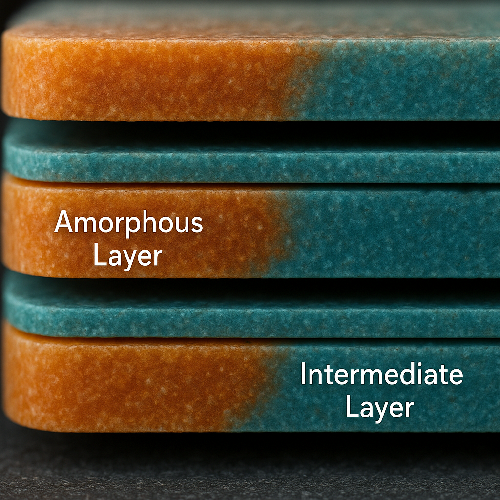
Now, let’s talk about what this invention does that’s new and smart. The inventors figured out a way to stack many thin amorphous layers, with a very thin “intermediate” layer in between each one. These intermediate layers are made from special two-dimensional materials—like molybdenum disulfide, graphene, or hexagonal boron nitride—that don’t react much with the layers above and below them.
Here’s how it works in simple terms:
First, you grow a thin amorphous layer (for example, amorphous boron nitride) on top of a base, called a substrate. This layer is thin enough so it stays in the jumbled, non-crystal state. Next, you put down a super-thin barrier, the intermediate layer. This can be as thin as one nanometer (that’s about 100,000 times thinner than a human hair!). This layer is made using materials that are flat at the atomic level, like graphene or molybdenum disulfide.
After that, you add another thin amorphous layer on top of the intermediate layer. You keep repeating this—amorphous layer, barrier layer, amorphous layer, and so on—until you have as many layers as you need. The key is that each amorphous layer is thin enough to stay jumbled and not turn into a crystal, even though the whole stack can be very thick.
The result? The entire stack keeps its low-dielectric constant, even as it gets thicker. The intermediate layers don’t just stop atoms from lining up; they also don’t add much to the overall dielectric constant, because they are very thin and have a similar or even lower dielectric constant themselves.
Let’s break down the main ideas and what makes this invention special:

1. Stacking method keeps layers amorphous: By using thin amorphous layers and separating them with two-dimensional material barriers, the stack never gets thick enough in one go for the atoms to line up. This stops crystallization and keeps the dielectric constant low.
2. Carefully chosen materials: The amorphous layers are made from elements like boron, nitrogen, silicon, carbon, or oxygen. The intermediate layers are from a group of materials known for being atomically flat and not reacting much, like graphene, black phosphorus, or transition metal dichalcogenides (such as molybdenum disulfide).
3. Thickness and dielectric constant control: Each amorphous layer is much thicker than the intermediate layer, but still thin enough to avoid crystallization. The difference in “dielectric constant” between the two types of layers is kept small, so the overall stack still blocks electricity well.
4. Scalable for real devices: The invention allows for five or more layers, with an overall thickness of 50 nanometers or more. This is enough for practical use in chips and wiring in real electronic devices.
5. Easy to make: The process uses standard chip-making methods, like plasma-enhanced chemical vapor deposition (PECVD) and atomic layer deposition (ALD). This means factories can make these stacks without having to build new machines.
6. Maintains low dielectric constant: Even when the overall thickness is high, the dielectric constant stays at 2.5 or below. In tests, stacks made this way kept their insulating power, while simple thick layers did not.
The invention can be used in all kinds of electronics. For example, it can go around the tiny metal wires inside chips to stop signals from leaking and slowing things down. It can also be used as a barrier layer to stop metals from spreading into the rest of the chip. And because it uses materials that are common and methods that factories already have, it can be adopted quickly.
To make the stack, you do the following:
– Put down a thin amorphous layer on your base.
– Add a super-thin intermediate layer using two-dimensional material.
– Repeat these steps as many times as needed to get the right thickness.
– Make sure each layer stays thin enough to be amorphous, but the whole stack can be thick.
The inventors also show that if you use the wrong material for the intermediate layer, or make it too thick, the dielectric constant goes up and you lose the benefit. So, picking the right materials and keeping the intermediate layer ultra-thin is key.
Tests showed that with this design, even very thick stacks keep the same low-dielectric constant as a single thin layer. That’s a big deal for chip makers, who can now make better, faster, and smaller electronics.
Conclusion
This new stacked structure is a simple but powerful idea. By carefully layering thin amorphous materials with two-dimensional barriers in between, the inventors have found a way to keep the good properties of thin insulating layers, even when the stack is thick. This solves a big problem in making tiny, fast electronics. With easy-to-find materials and standard production techniques, this invention is ready to help the next generation of devices run faster, cooler, and more reliably. Companies looking to make better chips and gadgets should pay close attention—this is a practical solution to a very real market need.
Click here https://ppubs.uspto.gov/pubwebapp/ and search 20250220809.