
Invented by AHN; Byeongseong, Song; Siho, Doh; Jiseong, Jeong; Jaehoon, Shin; Seunghyun, SAMSUNG ELECTRONICS CO., LTD.

Semiconductors power nearly every electronic device in our lives. Making them is a complex process, and even a tiny defect can mean a chip does not work. A new patent application presents a way to find and predict these defects using smart computer models. In this article, we break down what this patent is about, why it matters, where it fits in the world of semiconductor manufacturing, and what makes the invention special.
Background and Market Context
Semiconductors are the building blocks of modern technology. They are in our phones, cars, computers, and even home appliances. Companies spend a lot of money and time to make sure these chips work well. As chips get smaller and more powerful, making them becomes harder. A single small mistake in how they are made can cause the whole batch to fail.
The process to make a semiconductor chip involves many steps. Each step must be just right. There are machines that lay down tiny wires, add special materials, and carve out shapes at a scale too small to see with the eye. Sometimes, small things go wrong—like a tiny particle landing on the chip, or a step going a little too long or too short. Even a small slip can make the chip not work. Finding out what went wrong is very hard.
Right now, companies use many tools to check their chips. They might use special microscopes or cameras to look for defects. They also use computers to simulate how chips should look if made perfectly. But when a chip has a problem, it can be very hard to figure out what caused it. The process often takes a long time, and it can be expensive. This is a big problem for chip makers, because every minute counts and every bad chip loses money.
The market for semiconductors is huge and always growing. New phones, computers, and cars all need chips. The world wants more chips, and it wants them to be better, faster, and cheaper. But as chips get more complex, finding and fixing problems gets harder. This is why companies are looking for better ways to spot defects and fix them quickly.
If companies can predict when and why defects happen, they can save a lot of time and money. They can make better chips, faster. They can also make their factories run more smoothly. This is why there is so much interest in new tools and methods to inspect chips and their manufacturing processes. The patent application we are discussing focuses on a new way to use computer models to find and predict defects quickly and more accurately than before.
Scientific Rationale and Prior Art
To understand what is new about this patent, let’s first look at how chip inspection and defect detection works today.
In the past, chip makers checked for problems by using special microscopes. They would take pictures of chips and compare them to what a perfect chip should look like. If they found something strange, like a line that is too thick or a spot that is not supposed to be there, they would mark it as a defect. Some machines use lasers or electron beams to look inside chips, while others look at the surface.
Computer models are also used. These models, called simulations, try to predict what a chip will look like after each step of the process. If you know what should happen, you can compare it to the real chip and see if something is wrong. But these models are only as good as the data you give them. If you do not know all the things that can go wrong, or if you do not know the exact steps taken, the model might not help much.
More recently, companies have started using machine learning and artificial intelligence (AI) to find defects. These computer programs can learn from lots of data. They can look at many images and learn what a defect looks like. Some machine learning models, like artificial neural networks (ANNs) or convolutional neural networks (CNNs), can find patterns that people might miss. These programs can be trained on images of good chips and bad chips, then used to spot defects in new chips.
However, there are still problems. One big problem is that AI models can be a “black box.” They might tell you something is wrong, but they can’t always explain why or how the defect happened. Some models need a lot of data and a lot of computer power to work well. Also, current models often just tell you that a chip is bad, but not what caused the problem. If you don’t know the cause, it’s hard to fix it.
Previous patent filings have described using image comparison, simulation models, and even machine learning for defect inspection. Some methods look at chip images and compare them to a “golden” standard. Others run simulations to predict what should happen. Some use AI to classify images as good or bad. But these methods often work separately. They might not connect real chip measurements, computer simulations, and suspected defect causes in a single, easy-to-use framework.
In summary, current tools can spot defects, but they often cannot quickly, clearly, and automatically link real chip problems to their exact causes. This slows down the process and makes it harder to improve manufacturing. There is a need for a tool that can bring together real chip data, smart computer simulations, and machine learning to not just find defects, but to tell you what likely caused them and when they happened.
Invention Description and Key Innovations
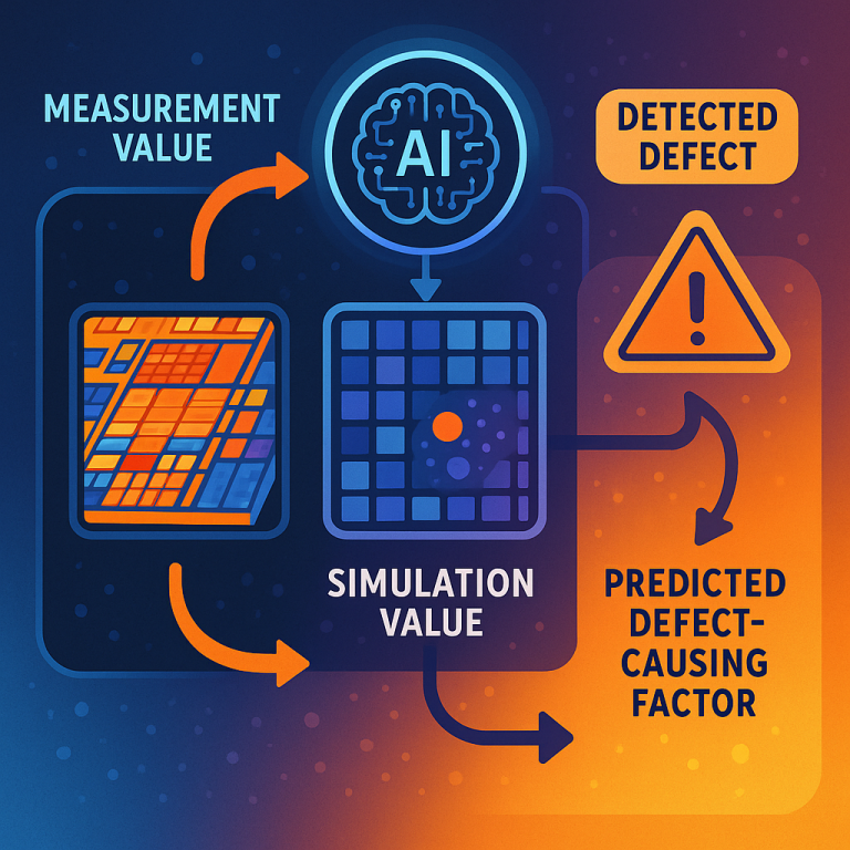
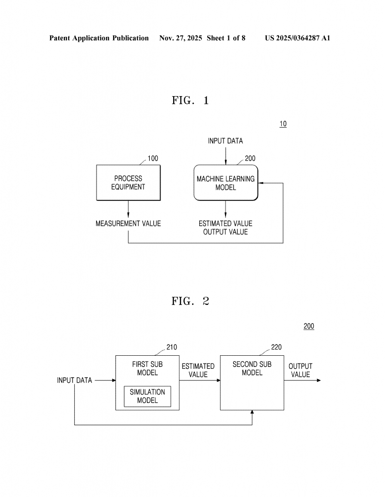
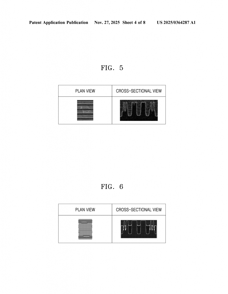
The patent application introduces a new way to inspect semiconductor chips using a blend of real-world measurements, computer simulations, and machine learning. The process starts with measuring a real chip. This could mean taking a picture of the chip from the top, from the side, or even slicing it and looking at the inside. These images or measurements are called the “measurement value.”
Next, the system uses a simulation. It builds a “virtual chip” using computer models. The simulation can include all the steps used to make the chip, and it can also include guesses about what might have gone wrong—these are called “suspected defect-causing factors.” For example, the simulation might try adding a small particle at a certain step, or changing the timing of a process, or making a line a little wider or narrower. The result is a simulated image or measurement of what the chip would look like if that suspected problem happened.
The real magic happens when the system compares the real chip measurement to the simulated ones. It uses machine learning, such as artificial neural networks or convolutional neural networks, to see how similar the real chip is to each virtual scenario. The computer can quickly test many different possible causes and see which one matches the real defect the best.
If the real chip matches a simulated chip with a certain problem—like a particle in a certain spot at a certain time—the system can tell you, “This defect was probably caused by a particle landing during this process step.” This gives engineers direct feedback, not just that a chip is bad, but why it is bad and how it likely happened.
The method also includes tools for making the comparison work better. For example, it can detect the boundaries in chip images using simple computer vision tools, like gradient filters. This helps the machine learning model focus on important features. The system can handle many kinds of input data, including images from optical microscopes or electron microscopes, and it can compare different views—top, side, or cross-section. This makes it flexible.
One key innovation is that the system does not just look for defects, it predicts the causes. It links the manufacturing steps, the possible problems, and the measured results all together. This helps engineers fix problems faster. If a chip fails, they can quickly find out if it was a particle, a timing error, or something else, and at which point in the process it happened.
Another important feature is that the system can rank possible causes by how similar the simulated defect is to the real defect. This means it does not just pick one answer—it can give a list, sorted by likelihood, helping engineers focus on the most likely problems first.
The whole process can be automated, saving time and money. It can also get smarter over time, as more data is collected and the machine learning model is trained further. This makes the system better at spotting new types of problems and giving better predictions.
The invention also fits easily into current manufacturing lines. It can use standard measuring tools and computer systems. The method can be used for different kinds of chips and adapted for new manufacturing steps as technology changes.
In summary, the main innovations are:
– Combining real chip measurements with flexible computer simulations that can try different suspected problems.
– Using machine learning to find which simulated problem matches the real defect.
– Automatically predicting the most likely cause and the process step where it happened.
– Allowing for automated, fast defect analysis, which saves time and helps engineers fix problems quickly.
– Adapting to different chip designs and manufacturing setups, making it useful for many companies.
This new approach goes beyond simply spotting bad chips—it helps answer the crucial question: “Why did this chip fail, and how can we stop it from happening again?” By making this process fast and smart, semiconductor makers can improve yields, lower costs, and bring better products to market faster.
Conclusion
Semiconductor manufacturing is getting more complicated every year, but the need for fast, accurate defect detection has never been greater. The patent application we have explored shows a smart, modern answer to this problem. By blending real-world measurements, powerful computer simulations, and advanced machine learning, the invention helps chip makers not just find bad chips, but understand why they are bad—quickly and clearly.
This system fits right into the real world of chip manufacturing, using current tools and data, but adding a layer of intelligence that can make a huge difference in speed, cost, and quality. As the demand for better chips grows, innovations like this will become essential. Companies that can quickly find and fix the root causes of defects will have a strong advantage in the fast-moving world of electronics.
If you’re in the semiconductor industry, understanding and applying these ideas can help you stay ahead. This patent represents a big step forward in making chip production smarter, faster, and more reliable.
Click here https://ppubs.uspto.gov/pubwebapp/ and search 20250364287.