Invented by CHOI; Chulmin, KIM; Sanghoon, BAIK; Seungjae, LEE; Jaeduk, Samsung Electronics Co., Ltd.
In this article, we will break down a new semiconductor device patent that introduces an improved way to make 3D memory chips more reliable and efficient. This patent centers around the use of a hydrogen-rich layer inside memory cell structures. We’ll look at why this matters, what problems it solves, and how it fits into current technology.
Background and Market Context
The way we use data has changed a lot. People and businesses need more and more storage, whether it’s for phones, computers, or big data centers. To keep up, chip makers have moved from flat, two-dimensional (2D) memory chips to three-dimensional (3D) ones. This shift lets them put more memory cells in the same area, making it possible to store much more data without making chips bigger.
These 3D memory chips are found in solid-state drives (SSDs), smartphones, and cloud servers. They are the backbone of everything from fast web browsing to artificial intelligence. As we store more data, the need for reliable and high-performing chips grows.
But packing more memory into smaller spaces brings challenges. When you stack cell layers higher and higher, tiny problems inside the chip can become big headaches. For example, making sure every memory cell works the same and doesn’t break down over time is hard. One issue that comes up is keeping enough hydrogen in the right places as chips are built. Hydrogen helps the cells work well, but as more layers are added, it becomes harder to get hydrogen where it’s needed. Without enough hydrogen, memory cells can become unreliable, leading to data loss or chip failures.
To solve these problems, engineers and inventors keep looking for new ways to make chips better. The patent we’re discussing introduces a special hydrogen-rich layer that helps address these reliability issues, especially as memory chips get more complex and layered.
Scientific Rationale and Prior Art
To understand why this invention is important, we need to know a bit about how memory chips work and what other solutions have been used before.
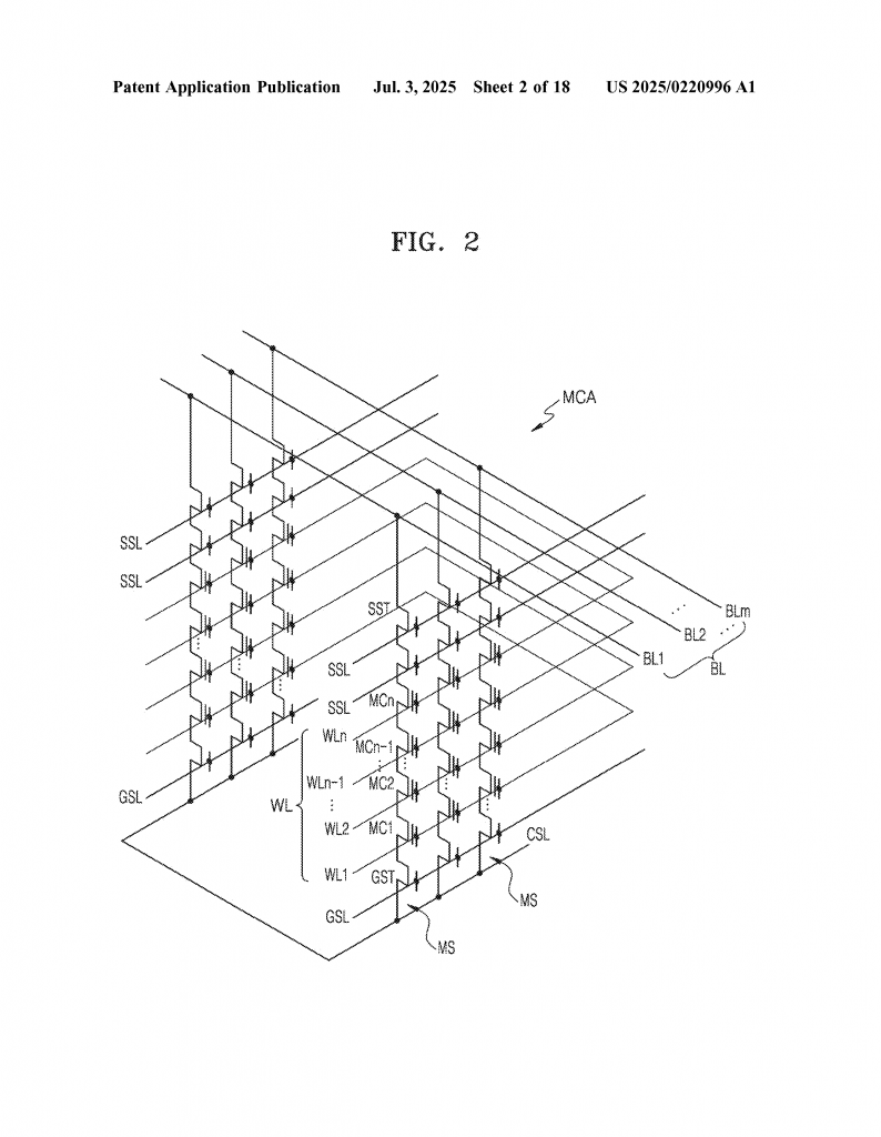
Most modern memory chips use what’s called NAND flash memory. In these chips, memory cells are tiny structures that can store electrical charges, representing data as 0s and 1s. In older 2D chips, these cells are laid out flat. But in 3D chips, they are stacked on top of each other, like floors in a tall building.
Each memory cell has several key parts: gate electrodes (which control whether the cell stores a 0 or 1), channel structures (where the current flows), and insulating layers (which keep signals from leaking). One important step in making these chips is making sure that the channel structure, which runs up through all the layers, is healthy and free of defects. Hydrogen is often used during manufacturing because it can fix certain types of defects, making the chips work better and last longer.
However, as chip makers build higher and higher stacks of memory cells, it gets harder for hydrogen to reach the deepest layers during manufacturing, especially when high temperatures are involved. If not enough hydrogen gets to where it’s needed, the cells might not work as well, leading to problems like faster data loss or chip breakdown.
In the past, chip makers tried to add extra hydrogen during different steps in the process, or used materials like silicon nitride (which can hold hydrogen) as protective layers. Some patents have described using deuterium, a form of hydrogen, which is even more stable at high temperatures. Still, these approaches could not guarantee that every part of the chip, especially the deepest layers, would get enough hydrogen. With every new generation of 3D chips, the problem became worse.
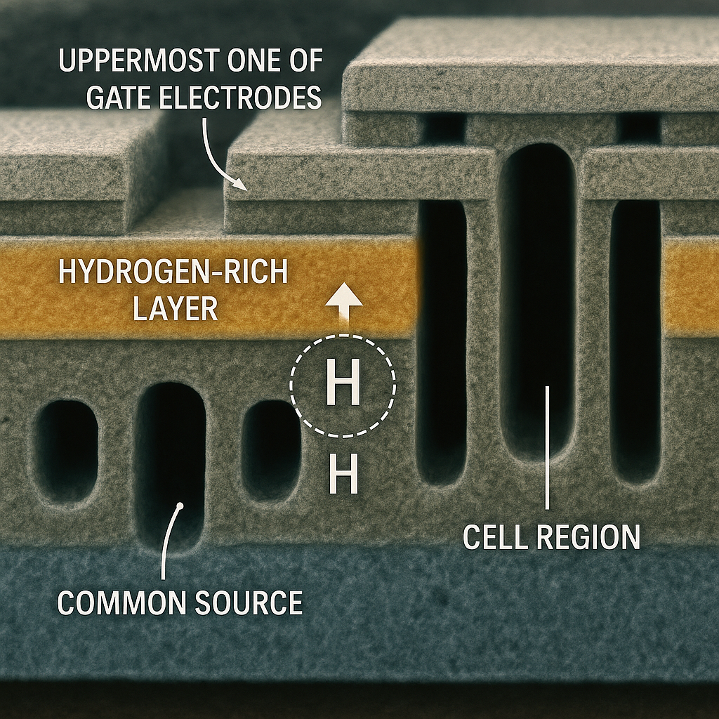
What sets this new patent apart is that it puts a hydrogen-rich layer in a very specific place inside the cell structure, right where the memory cells meet the common source layer. This targeted approach helps make sure that hydrogen is present where it’s most needed, even during high temperature steps, and even as chips get more and more complex.
Invention Description and Key Innovations
Let’s take a closer look at what the patent claims and what makes it different from earlier solutions.
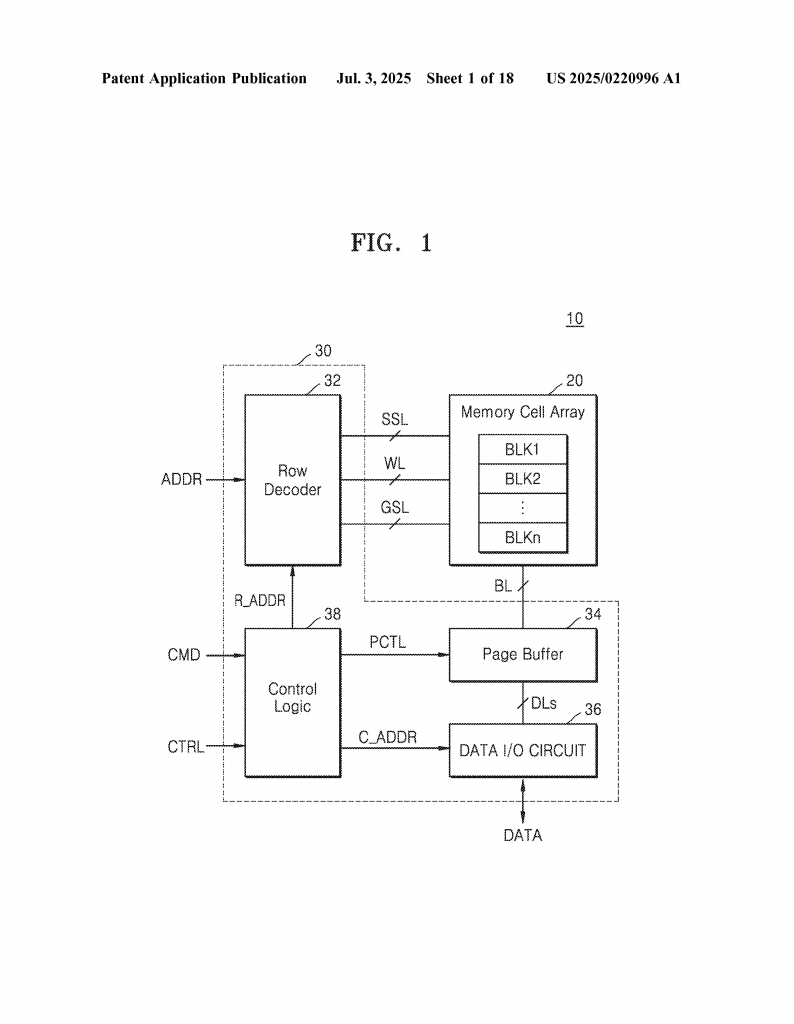
The new device is a 3D semiconductor memory chip. It has two main parts: a periphery circuit structure, which handles things like controlling the chip and moving data in and out, and a cell structure, which is where the actual data is stored.
Inside the cell structure, there are several regions:
– The cell region holds the stacked memory cells.
– The connection region helps link the cells to the circuits that control them.
– The periphery circuit connection region connects the memory cells to the periphery circuits.
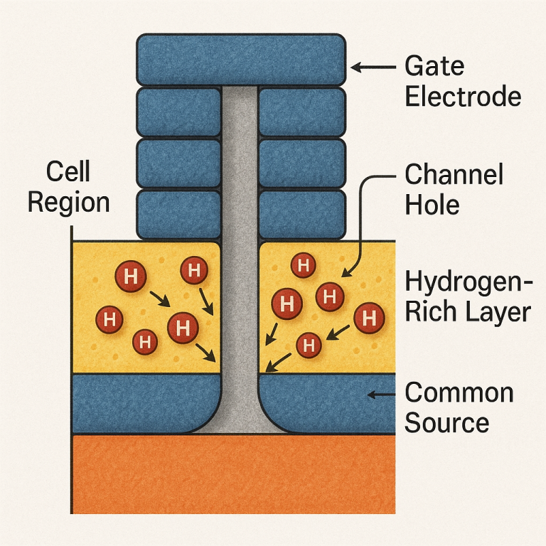
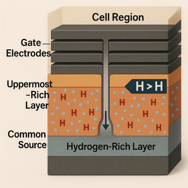
The main innovation is the placement of a hydrogen-rich layer between the uppermost gate electrode and the common source layer in the cell region. This layer is much richer in hydrogen (and possibly deuterium) than the other parts of the chip, such as the gate electrodes. In some versions, this layer is made of silicon nitride, a material that is good at holding hydrogen.
Here’s why this is important:
– Hydrogen delivery: During chip manufacturing, especially when the process gets hot, hydrogen can escape or fail to reach deep layers. This new hydrogen-rich layer acts as a reservoir, releasing hydrogen exactly where it’s needed to fix defects in the memory cells.
– Improved reliability: With more hydrogen available, memory cells are less likely to develop problems that would make them lose data or stop working. This is especially helpful as chips get taller, with more layers.
– Flexibility: The patent describes that the hydrogen-rich layer can include both hydrogen and deuterium, or just deuterium. Deuterium is less likely to escape during high heat, so it can be even better for stability.
– Specific concentration: The hydrogen-rich layer is at least 1% (and in some cases, more than 20%) richer in hydrogen than the surrounding layers. This ensures a real, meaningful boost in hydrogen supply.
– Thickness and placement: The patent specifies that this layer is just 50 to 500 angstroms thick. It sits directly on top of the uppermost gate electrode and is covered by the common source layer. In some versions, the channel structures even penetrate this hydrogen-rich layer, helping hydrogen reach deeper into the cell.
– Structures and shapes: The patent also describes the shapes of the channel structures, which can be cylindrical or trapezoidal, and how they connect to the periphery circuits for best performance and manufacturability.
– Compatibility with modern manufacturing: The invention is designed to fit into the process flows already used in advanced chipmaking. The hydrogen-rich layer can be deposited using standard methods, and doesn’t require big changes to the manufacturing line.
The patent also covers how to make these chips, including the steps of stacking the cell region on the periphery circuit, forming the hydrogen-rich layer, building the gate electrodes, creating the channels, and connecting everything together. These steps are laid out so that the hydrogen-rich layer is always in the right place to do its job.
The result is a memory chip that is more reliable, especially as manufacturers keep adding more layers to boost capacity. This is a direct answer to the problems faced in pushing 3D NAND technology to new heights.
Conclusion
This patent offers a practical, targeted solution to a real problem in the world of advanced memory chips. By putting a hydrogen-rich (and possibly deuterium-rich) layer right where it’s needed, the inventors have found a way to keep 3D memory chips reliable, even as the technology becomes more complex. This means better, longer-lasting storage for everything from everyday gadgets to giant data centers.
As memory chips continue to evolve, solutions like this will be key in making sure we can keep up with the world’s growing need for data. This invention is a great example of how small changes in chip design can lead to big improvements in performance and reliability.
Click here https://ppubs.uspto.gov/pubwebapp/ and search 20250220996.