Invented by Maeng; Jun Young, Park; Jae Woo, Baek; Seung Yeob, Kwak; Myoung Bo
In the world of electronics, how we move information from the real world into a computer or digital device matters a lot. This article will help you learn about a new type of sample-and-hold circuit, as described in the patent application above, that is designed to make those conversions faster and more reliable. We’ll break down why this matters, what science came before, and what new ideas this invention brings. Let’s get started!
Background and Market Context
Modern devices are hungry for data. Every year, the amount of information we send and process grows. Phones, computers, and communication systems are always looking for ways to send information quicker and with fewer mistakes. That’s why the circuits that help move signals from the outside world into digital form are so important.
At the heart of this process is the analog-to-digital converter, or ADC. Think of an ADC as a tiny translator: it listens to the world of sound, light, or radio waves, then turns those wavy signals into numbers a computer can understand. The ADC can only do a good job if the signals it hears are clear and steady. Before an ADC does its work, it often relies on a helper circuit called a sample-and-hold circuit. This helper grabs a quick sample of the signal and holds it still, just for a moment, so the ADC can read it.
As devices get faster—think about how much quicker your phone is now compared to ten years ago—the job of these circuits gets harder. The signals can get weaker and less clear as they move through wires, especially as we push for ever higher speeds in things like high-speed internet connections or wireless networks.
To make things even trickier, these circuits are built from tiny electronic parts that can change how they act depending on the temperature, the power voltage, or even small differences from one chip to another. This is called PVT variation (process, voltage, temperature). If a circuit isn’t designed to handle these changes, your device might not work as well, or it might even make more mistakes as it gets hot or cold, or as the battery drains.
All this means that companies and engineers are looking for new and better ways to design these “sample-and-hold” circuits. They want circuits that work fast, are strong against these small changes, and don’t mess up the signal before it gets digitized. This is where the invention in the patent application comes in—it’s trying to solve these exact problems for next-generation electronics.
Scientific Rationale and Prior Art
To understand the value of this new sample-and-hold circuit, it helps to know what’s come before. Traditional sample-and-hold circuits often use simple electronic switches and capacitors. When a signal comes in, a switch closes for a tiny moment, letting the capacitor grab and store the voltage. Then, the switch opens, and the capacitor holds the voltage steady so the ADC can read it.
But there are problems with older designs. One big issue is common mode voltage. This is a kind of “average” voltage that can drift up or down because of changes in power supply, temperature, or how the circuit was made. If this common mode voltage isn’t kept steady, the ADC can get confused, leading to errors or more noise in the digital data.
To keep the common mode voltage steady, older circuits sometimes use passive parts like resistors or capacitors. These are simple parts that don’t need power to work. They can help, but there’s a catch: they can slow down how quickly the circuit responds. When you want ultra-fast conversion—think of high-speed data connections or advanced wireless networks—this slow-down becomes a big problem.
Other designs try to use special feedback circuits, where the circuit watches its own output and makes small changes to keep things steady. Some use operational amplifiers (op-amps) to help with this feedback. But feedback circuits can be hard to design well. If the feedback is too slow, it doesn’t help. If it’s too fast, it can cause the circuit to become unstable and even create more noise. Managing the feedback so it’s “just right” is a delicate art.
There are also designs that use multiple channels, called time-interleaved ADCs. These break up the job among several smaller ADCs running in parallel, each taking turns. This can help boost speed, but only if all the channels are matched closely and the sample-and-hold circuits feeding them are rock-solid. If even one channel gets a noisy or shifted signal because of poor sample-and-hold design, the whole system can suffer.
In summary, the science and engineering behind sample-and-hold circuits has focused on:
– Grabbing signals quickly and holding them steady
– Keeping the common mode voltage stable
– Providing strong performance, even as chips get hot, cold, or change over time
– Working fast enough for new, high-speed data systems
– Avoiding extra noise or signal loss
But previous methods have struggled, especially at very high speeds and in the face of PVT variation. Circuits using passive parts can slow things down. More complex active feedback circuits can help, but are hard to get right and may still be sensitive to changes in temperature or power. This sets the stage for a new approach, which is exactly what this patent application presents.
Invention Description and Key Innovations
This invention brings a new way to design a sample-and-hold circuit, aimed directly at solving the problems we described above. Let’s walk through how it works and why it stands out.
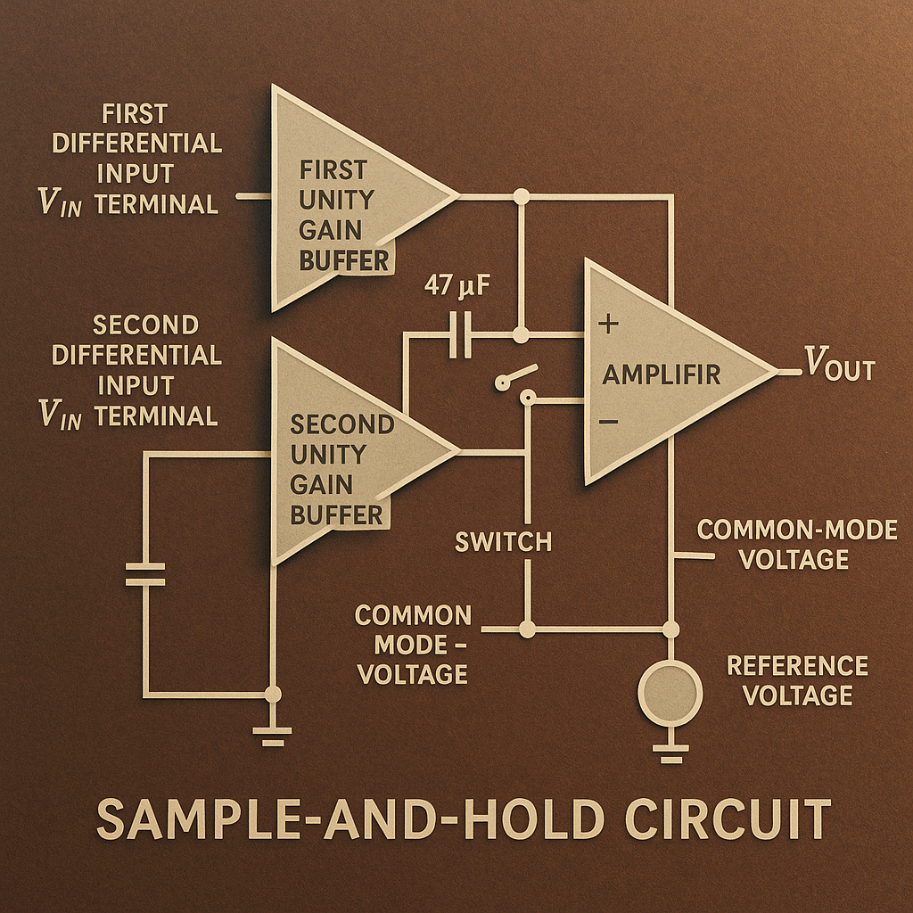
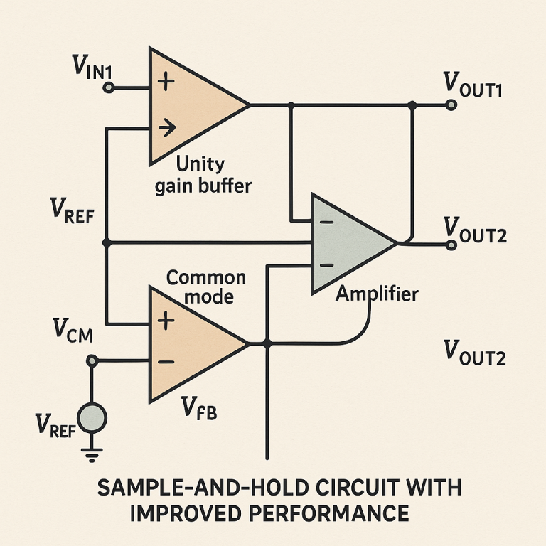
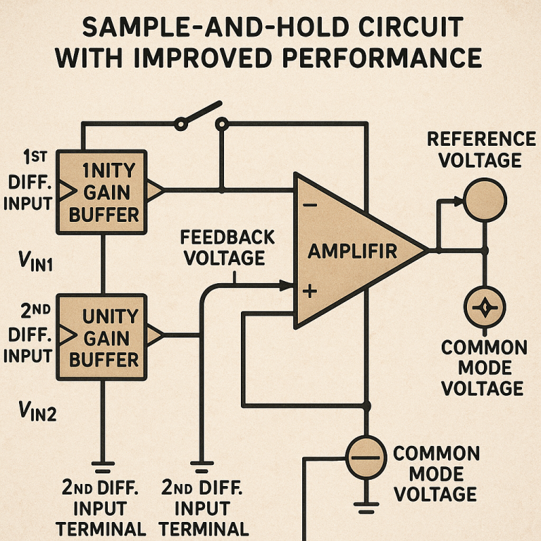
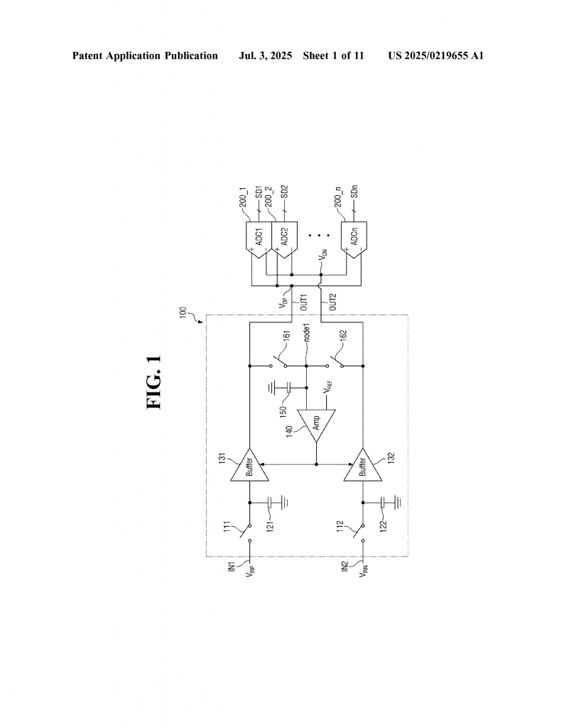
At the heart of this circuit are a few important building blocks:
– Differential input terminals: These are the entry points for the incoming signal. Using two inputs, instead of just one, helps cancel out noise and makes the circuit more robust.
– Unity gain buffers: These are special circuits that pass the input voltage to the output without changing the level (the gain is “1”). They act as strong helpers, making sure the signal isn’t weakened or changed as it moves through the circuit.
– Sampling switches and capacitors: These grab and hold a snapshot of the signal. The switches connect the input to the buffer for a brief moment, letting the capacitor store the voltage.
– Feedback amplifier: This is the “brain” of the circuit. It watches the outputs from the buffers, compares them to a steady reference voltage, and generates a feedback voltage. This feedback helps keep the circuit steady, even if things like temperature or power supply change.
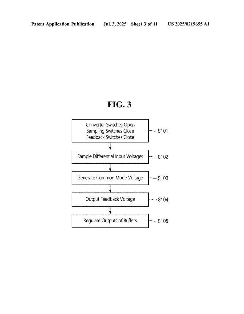
The key innovation here is how the feedback works. Instead of using slow passive parts, the circuit generates a common mode voltage directly from the outputs of the unity gain buffers. This voltage is compared to a reference, and the difference is amplified and sent back as a feedback voltage. The feedback voltage is used to control the unity gain buffers, making sure that their output stays steady and matches the reference as closely as possible.
This feedback loop helps the circuit automatically adjust itself if things change. If, for example, the voltage drifts up because the chip gets warm, the feedback will push it back down. If the process used to make the chip wasn’t perfect and changed the circuit’s behavior, the feedback fixes it. If the power supply wobbles, the feedback helps keep things on track.
Another smart feature is that the circuit can be extended to handle multiple channels. This is important for time-interleaved ADCs, where many channels are working in parallel. The same feedback mechanism can keep all channels tightly matched, so the whole system works smoothly and quickly, without any channel falling behind or going out of sync.
Let’s look at some specific technical features from the invention:
– The use of sampling and feedback switches allows the circuit to alternate between “sampling” and “holding” modes. When sampling, the circuit grabs the signal. When holding, it disconnects from the input and keeps the voltage steady for the ADC to read.
– The feedback capacitor stores the common mode voltage briefly, so the amplifier always has the right information even as the switches turn on and off.
– The feedback voltage can control the bias current in the unity gain buffers. This means the buffers can be quickly adjusted to match the reference voltage and cancel out any PVT variation.
– The design avoids using slow passive resistors or capacitors for extracting the common mode voltage. Instead, it uses active electronic switches and buffers for speed.
– The circuit can be expanded to more than two channels, and the feedback system can regulate all of them at once.
What does all this mean for real-world devices?
Devices using this sample-and-hold circuit can:
– Work faster, since there’s no slow-down from passive components
– Deliver cleaner, more reliable digital data to the ADC
– Stay steady and accurate even when temperature, power, or manufacturing conditions change
– Be used in high-speed communication systems, wireless devices, and advanced computing systems where performance is key
– Be easily expanded for systems that need many channels, like time-interleaved ADCs in 5G or high-speed networking gear
The invention is not just about making one part better—it’s about creating a smarter, more robust building block for the next generation of digital devices. Its feedback system is like a self-correcting mechanism that keeps everything on target, no matter what’s happening around it.
Conclusion
The world of electronics is always moving forward, and the circuits that help bridge the gap between the real world and the digital world are crucial to that progress. This new sample-and-hold circuit, as described in the patent application, brings together fast operation, strong feedback control, and flexibility for multi-channel systems. It solves the problems of signal drift, noise, and instability that have bothered older designs, especially in the face of changing temperatures, power supplies, or manufacturing quirks.
If you’re building devices that demand speed and accuracy—whether for communication, computing, or sensing—understanding and using this kind of sample-and-hold circuit could be a game-changer. It’s a great example of how smart engineering and clever feedback can push technology to new heights, making our devices faster, more reliable, and better able to handle the challenges of tomorrow.
Click here https://ppubs.uspto.gov/pubwebapp/ and search 20250219655.