Invented by CAVALLO; Francesca, UNM RAINFOREST INNOVATIONS
Today, we’re exploring a new and exciting patent application that brings together the worlds of optics, semiconductors, and modern computing. In this article, we’ll break down the key ideas and innovations behind a platform designed for spatial analog optical computing on a chip, or SAOC. We’ll keep things friendly and easy to follow, so you can understand how this technology could change the way we process information.
Background and Market Context
Let’s start with a simple question: what is computing, and why should we care about new ways to do it? Traditionally, computers use electricity flowing through wires and switches called transistors. These transistors are tiny, and millions of them fit on a chip. They control how numbers and information move, helping us do everything from sending texts to analyzing scientific data.
But as we keep shrinking these transistors, we’re running into problems. It gets harder to make them smaller, faster, or more energy-efficient. At the same time, people want computers to do more and more, using less power and taking up less space. This is where new ideas come in—like using light instead of electricity to do some of the work. Light, or optical signals, can carry information very fast and with very little energy loss.
Analog optical computing isn’t new. For decades, scientists have used big, table-sized setups with mirrors, lenses, and lasers to process information in unique ways. These setups can do things like sorting images, filtering signals, or even solving math problems—all by carefully shaping and guiding light. But these systems are too bulky for everyday use or for putting inside your phone or computer.
The challenge is to take these powerful optical tricks and shrink them down to the size of a chip. If we could do that, we could make computers that are much faster and use less power for certain tasks. This is especially important for things like artificial intelligence, image processing, and communications, where huge amounts of data have to be managed quickly and efficiently.
That’s why the market is excited about new platforms for spatial analog optical computing on a chip. This technology aims to bring the speed and efficiency of optical computing into a tiny, chip-sized format that can work alongside traditional electronic circuits. Startups, big tech companies, and research labs all over the world are racing to develop these systems, hoping to unlock new levels of performance and energy savings.
But there are big hurdles. The materials have to be just right. The way the light moves and interacts with the chip has to be carefully managed. And the manufacturing process has to be reliable and compatible with current chip-making factories. This patent application addresses these challenges head-on, proposing a new way to build and operate these optical computing platforms using well-known materials like germanium and graphene.
Scientific Rationale and Prior Art
To really appreciate this invention, we need to step back and look at the science and the work that came before. In analog optical computing, the main idea is to use the natural properties of light—how it bends, spreads out, or combines—to perform calculations. For example, passing a light wave through a special lens can automatically produce a mathematical operation called a Fourier transform. This is a key step in many types of signal and image processing.
Traditionally, these operations were done using lenses and mirrors made of glass, set up on a large optical table. While this works, it’s hard to make it small, stable, or easy to use in real-world devices. Researchers have long wanted to move these same kinds of calculations onto a chip, so they can work alongside tiny electronic circuits.
Over time, there have been many attempts to do this. One approach is to use materials whose optical properties can be controlled very precisely. These materials, called graded index (GRIN) media, can bend light in a way that mimics the action of traditional lenses, but on a much smaller scale. Another approach is to use metasurfaces—thin layers made up of tiny structures that can shape light in complex ways.
Some early chip-scale optical computing systems managed to do simple tasks, but they often faced problems. The materials were hard to make with the needed accuracy, or they absorbed too much light, wasting energy. Sometimes, the devices were too sensitive to small changes in the environment, or they couldn’t be made using standard chip-making techniques. Other times, the designs worked in theory but turned out to be very hard to build or operate reliably.

One big advance was the use of plasmonic materials, which can squeeze light into very small spaces and control it with high precision. Graphene, a single layer of carbon atoms, became a favorite because it can carry these special light waves (called plasmons) with low loss and can be tuned easily by applying a voltage.
Germanium is another important material in this field. It has good electronic properties and is already used in chip-making. It can also support the growth and use of graphene, making the two a good match for integrated devices.
Still, there were unsolved problems. Making the needed shapes and layers on the chip—especially with the right variation in thickness and composition—was tricky. Getting the materials to work together smoothly, especially at their boundaries, was also a challenge. And previous designs often couldn’t be made small enough, or didn’t work well with the standard processes used to make modern chips (known as CMOS compatibility).
This patent application builds on all this earlier work. It borrows ideas from optical tables, graded index media, metasurfaces, and plasmonics, but combines them in a new way. It also addresses the practical problems of making these structures on a chip, using methods and materials that fit with existing chip factories. By focusing on the details of how to make and control the different layers—especially the grooved and parabolic shapes, the use of graphene, and the metal backgate—it aims to deliver a platform that can perform real, useful optical computations at the chip scale.
Invention Description and Key Innovations
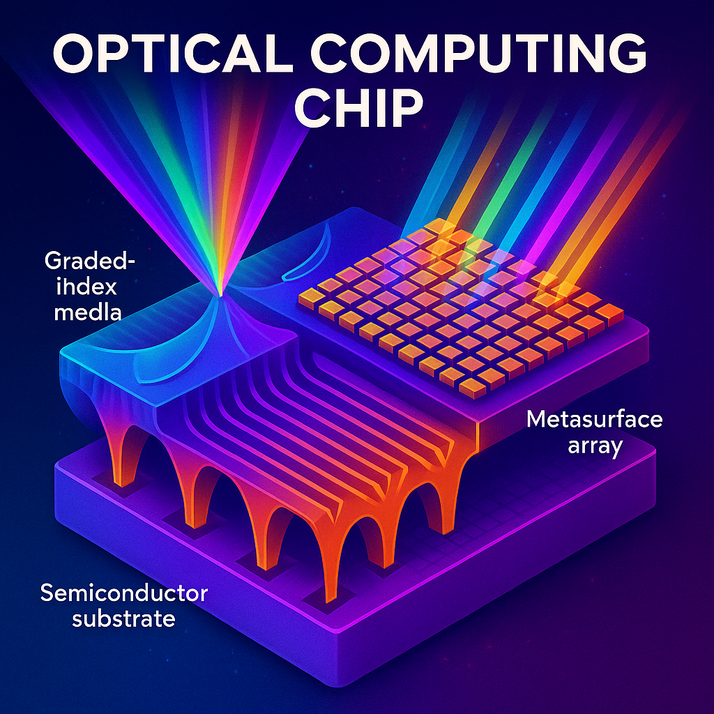
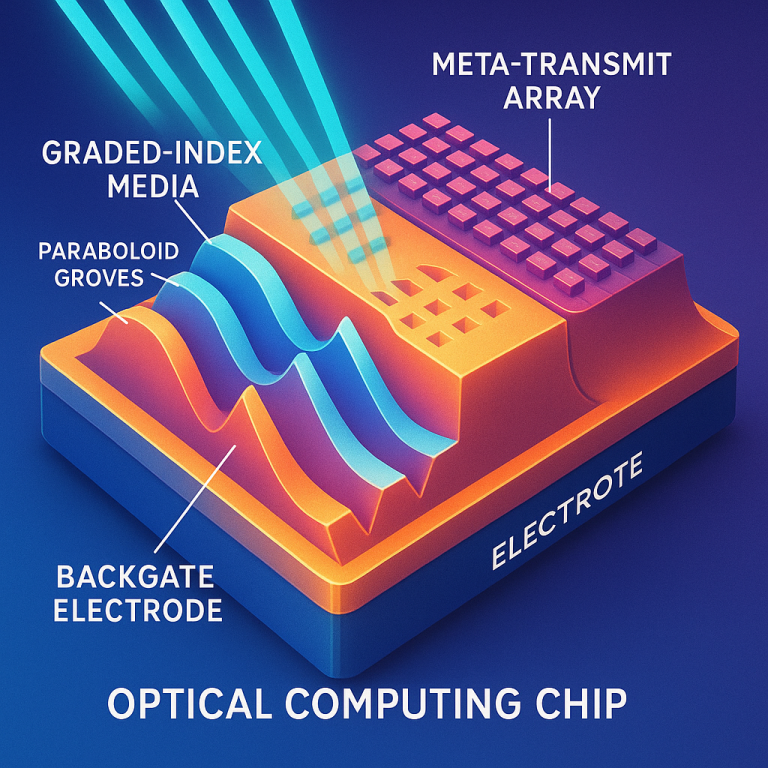
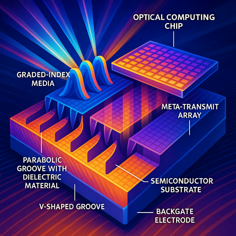
Now let’s get into the heart of the invention. The patent describes a new integrated computing platform that brings spatial analog optical computing onto a chip using a combination of germanium, graphene, and clever fabrication techniques.
The basic structure starts with a semiconductor substrate, often made of germanium. This forms the solid base of the chip. On the bottom of this substrate, a metal backgate electrode is added. This electrode is important because it lets you control the way electricity and light behave in the layers above by applying a voltage.
On the top side of the chip, special sections are made called graded index (GRIN) media. These are not flat—they have a carefully shaped, grooved surface. The grooves are made in a way that gives them a smooth, parabolic curve. This shape is key, as it lets the device bend and shape light in the needed way to perform operations like the Fourier transform. The GRIN media can include a dielectric layer (an insulating material), and on top of this, a layer of graphene is placed. The graphene is thin, strong, and very good at guiding and controlling light waves on the surface of the chip.
Right next to the GRIN sections sits a meta-transmit array (MTA). This is a kind of metasurface, made by patterning the top of the substrate in fine detail. The MTA can shape or filter the light even further, letting the system perform more complex mathematical operations. A layer of graphene can also be added on top of the MTA to help guide light and make the whole system tunable with electrical signals.
The backgate electrode on the bottom of the chip plays a special role. By applying a voltage, you can change how the graphene conducts electricity and light. This lets you tune the way the GRIN lenses work—making them more flexible and able to do different kinds of computations as needed. The voltage can be controlled by a circuit, so the chip can quickly switch between different modes or tasks.
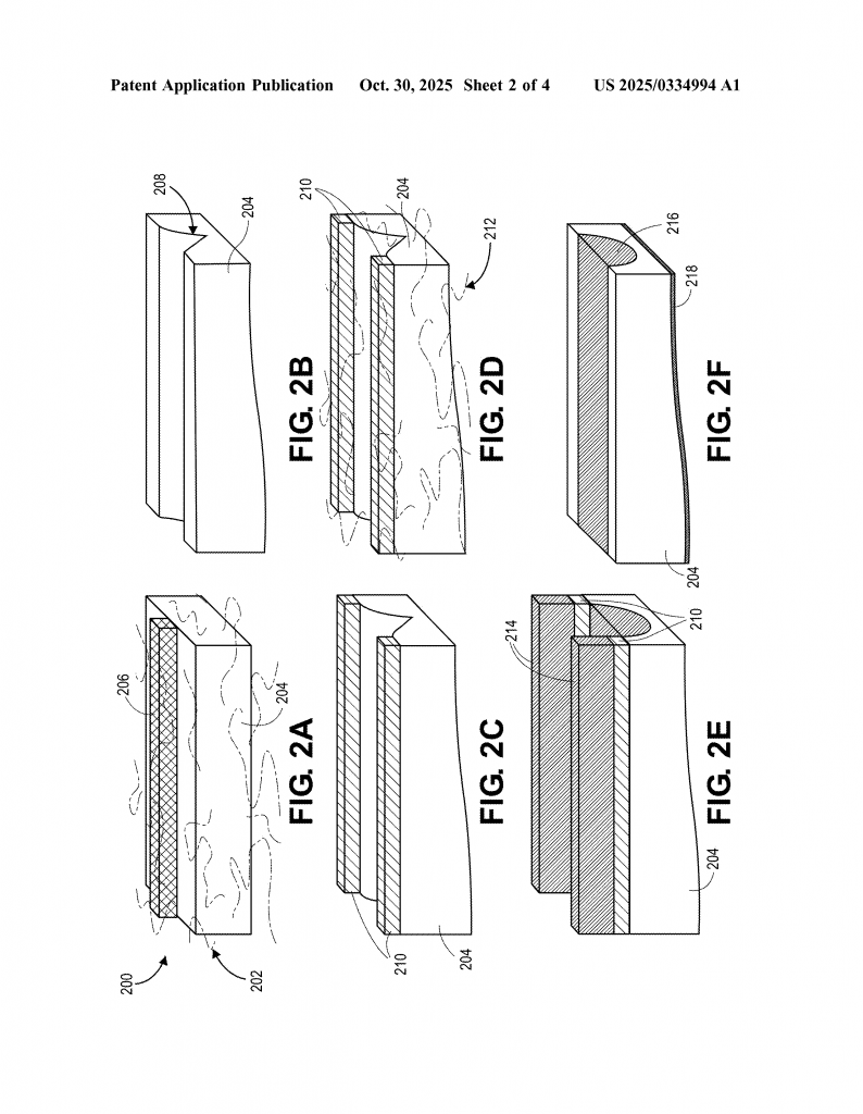
The patent also describes a step-by-step method for making the chip. The process starts with etching the top of the germanium substrate to create sharp, v-shaped grooves. These are then smoothed out using a water-based etching process to make smooth, paraboloid-shaped grooves. These grooves are filled with a dielectric material, such as a polymer or epoxy, using techniques like spin coating. This ensures that the dielectric fills the grooves evenly and cleanly.
Next, a graphene sheet is transferred from its growth substrate, usually a copper foil, onto the patterned surface of the chip. This is done using a polymer-assisted process to make sure the graphene lands in the right place and sticks well. After this, the back side of the chip is coated with metal using a process called physical vapor deposition, creating the backgate electrode.
The result is a chip with carefully shaped GRIN lenses and a meta-transmit array, all topped with a layer of graphene, and with a metal gate underneath. The structure can be tuned and controlled using electrical signals, and it can perform fast, low-power optical computations right on the chip.
This platform is designed to be compatible with current CMOS chip-making processes, making it easier to manufacture at scale. It also provides flexibility in the choice of materials for the dielectric and can be adapted for different types of computations by changing the shape or arrangement of the grooves and the MTA.
Some of the key innovations here include:
– The use of a parabolic profile in the GRIN media to smoothly control light for Fourier transforms and other operations.
– The integration of graphene layers for low-loss, tunable plasmonic waveguiding.
– A fabrication process that uses both anisotropic and isotropic etching to achieve the needed groove shapes.
– The use of a metal backgate electrode for electrical tuning of the chip’s optical properties.
– A platform that brings together all these elements in a compact, chip-scale form that fits with existing manufacturing methods.
All these features make the platform not just a clever scientific idea, but a practical solution for next-generation computing needs. It can be used for optical signal processing, fast data analysis, imaging, and communications. It could help power the next wave of artificial intelligence, data centers, or advanced sensors, all while using less power and taking up less space than traditional approaches.
Conclusion
The invention described in this patent application offers a clear path forward for bringing optical computing into the mainstream. By combining the unique properties of germanium, graphene, and carefully-shaped dielectric layers, and by using a process that fits with modern chip factories, it addresses many of the big challenges that have held back chip-scale optical computing.
This platform is flexible, efficient, and scalable. It’s designed to work with existing technology, but also pushes the boundaries of what’s possible in computing. As demand grows for faster, smaller, and more energy-efficient computers, solutions like this will become more and more important.
If you’re interested in the future of computing—whether you’re an engineer, a researcher, or just a tech enthusiast—this is a development to watch. It brings us a step closer to a world where light and electricity work side by side, powering new kinds of devices and applications we’re only beginning to imagine.
Click here https://ppubs.uspto.gov/pubwebapp/ and search 20250334994.