Invented by PENG; Hede, WU; Hanzhen, Samsung Semiconductor China Research & Development Co., LTD


Wireless technology moves fast. Every new phone, tablet, or smart device tries to be faster, use less battery, and work better in tough places like crowded cities or inside buildings. But as these gadgets get more advanced, the parts inside them — especially the parts that send and receive signals — get a lot more complex. Today, we’ll explore a new patent application for a wireless communication device that promises to make these gadgets cheaper, simpler, and better at handling all those signals flying through the air.
Background and Market Context
If you use a smartphone, wear a fitness tracker, or even drive a smart car, you already depend on wireless communication every day. These devices talk to each other and to the internet using tiny antennas and powerful chips that turn your voice, text, or video into radio waves and back again. Over the last few years, as 5G networks rolled out, these devices needed to handle more data, connect to more types of networks, and work in more places. That means they needed more antennas, more chips, and more complicated ways to switch between different signal paths.
But here’s the problem: Packing all those antennas and signal paths into a small device is expensive. The more parts you need, the more money it costs to build the device. Not only that, but each extra switch or wire can make the signal weaker — imagine trying to talk to someone through a long tunnel. If the signal gets too weak, your phone drops calls or slows down. Plus, the more complex the inside of the phone is, the harder it is for engineers to design and fix, and the more battery it uses.
For companies making these gadgets, the pressure is huge. They need to support all the latest features (like 5G, 4G, WiFi, and Bluetooth) while keeping the price low and the battery life high. Especially as the world moves to even faster wireless standards, making the inside of the device smarter — not just bigger or more crowded — is the key to staying competitive.
This is where the invention in the patent steps in. It offers a new way for the chips and antennas inside a device to talk to each other. The idea is to make switching between antennas and signal paths much simpler, with fewer parts and less power loss. That means cheaper devices, longer battery life, and better performance — all things that users and manufacturers want.
Scientific Rationale and Prior Art

Let’s get down to basics: At the heart of every wireless device is a chip called a radio frequency integrated circuit (RFIC). This chip turns your digital data (like your voice or a photo) into radio signals that can travel through the air. It also takes incoming signals and turns them back into data your device can use. The antennas are like ears and mouths for your device, sending and catching those radio signals.
In older designs, the RFIC connects to several antennas through a set of switches. If your device wants to use a different antenna (maybe because you’re holding your phone a certain way or moving to a different room), it flips these switches to pick the best one. This process is called “antenna diversity” or “antenna switch diversity” (ASDiv). It helps the device pick the antenna that gets the best signal.
The trouble is, these switches are often big, complex, and expensive. Imagine a railroad with dozens of tracks and lots of levers — every extra switch adds cost, space, and a chance for the signal to get weaker. In many current devices, the RFIC sends its signal to a big “antenna switch module” with lots of these switches. The more antennas and signal paths you want, the more switches you need. This creates a web of connections that can get messy fast.
To make matters worse, every time a signal passes through a switch, some of its strength is lost. This is called “insertion loss.” Too much loss means dropped calls, slower data, or weaker WiFi. In high-end smartphones, engineers have spent a lot of time and money trying to reduce this problem, but the solutions often involve even more complicated hardware.
Previous patents have tried to improve things by making smarter switches, using better materials, or adding even more antennas. Some have moved certain switching functions onto the RFIC itself, but usually only for simple cases. Bigger switches (like four-pole four-throw, or 4P4T switches) are still needed outside the main chip, especially when you want to support both 4G and 5G, or have more than two antennas. These big switches are costly, take up space, and are hard to control.
What sets the new patent apart is how it splits up the jobs: It puts a smart, flexible switching module inside the RFIC, and uses simpler, cheaper switches outside the chip to connect to the antennas. This setup makes it easier for the device to switch between different antennas or signal paths with fewer switches, less signal loss, and lower cost. It also gives engineers more freedom to design devices for new ways of using networks, like switching between 4G and 5G without needing lots of extra hardware.
Invention Description and Key Innovations


Now let’s break down what the new device actually does, in plain language.
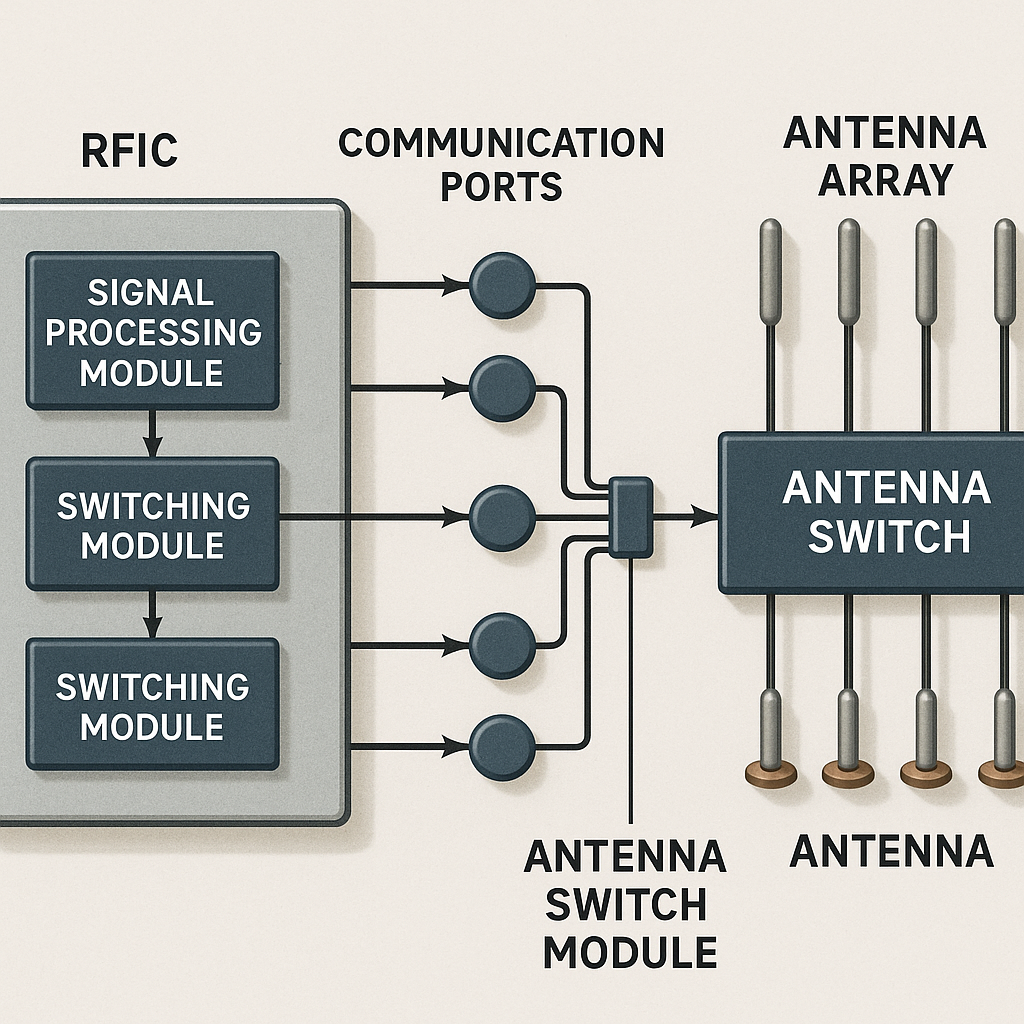
Inside the device, there’s a main chip — the RFIC — with several parts. These include:
Signal Processing Modules: Think of these as tiny helpers that get a signal ready to be sent out, or that clean up a signal coming in. There can be two, three, four, or more of these, depending on how many antennas and features the device supports.
Switching Module: This is the “brain” that decides which signal processing module connects to which communication port. It sits inside the RFIC. Instead of having all the switching outside the chip (where it’s more expensive and less efficient), the smart switching happens right here, close to where the signals are created or received.
Communication Ports: These are like doors leading from the RFIC to the outside world. Each port can send signals to, or receive signals from, the antennas. Some ports are for sending (TX), some for receiving (RX), and some do both (TRX).
Antenna Switch Module: This sits outside the RFIC. It’s made up of simple switches (like double-pole double-throw, or DPDT switches) that connect the communication ports from the RFIC to the antennas. Each switch can connect a port to one of two antennas, making it easy for the device to pick the best antenna for the job.
Antenna Array: This is a group of antennas, often organized into groups (like “Group 1” and “Group 2”), each covering specific frequency bands (like 4G or 5G).

What’s new here is how these parts work together. The switching module inside the RFIC lets any signal processing module connect to any communication port. This means the device can quickly switch between sending on one antenna to sending on another, or even switch between 4G and 5G, without needing a big, expensive switch outside the chip.
For example, say your device wants to switch from using Antenna 1 (for 5G) to Antenna 2 (for 4G). The switching module inside the RFIC makes this change, then tells the simple antenna switch module outside the chip to connect the right port to the right antenna. Because the big, complex switching is now inside the chip, the outside switches can be much simpler and cheaper.
This new setup has lots of benefits:
Lower Cost: Fewer big switches mean the device is cheaper to make.
Less Signal Loss: Fewer connections and shorter signal paths mean your calls and data stay strong.
More Flexible Design: Engineers can easily add or change antennas or support new wireless standards without redesigning the whole signal path.
Better Performance: The device can switch between antennas quickly, pick the best one for the environment, and handle both 4G and 5G at the same time.
Longer Battery Life: Less power is wasted in the signal path, so your device can last longer on a single charge.
The patent also covers special features like “Antenna Switch Diversity” (ASDiv) and “Sounding Reference Signal” (SRS) transmission. These are ways for the device to pick the best antenna for sending or receiving signals, depending on signal strength, interference, or other factors. By making it easy to switch antennas or signal paths, the invention helps the device always use the best option, giving you better call quality and faster data.
Another clever part: The system can handle both “independent” 5G (Standalone, or SA) and “non-independent” 5G (NSA, where 5G and 4G work together). This is important because many networks around the world use both at the same time. The new design can switch between these modes with just a few changes in the switching module, without needing extra parts.
Finally, the patent describes how this technology can be used in lots of devices: phones, tablets, wearables, vehicles, smart TVs, and more. Because it makes the inside of each device simpler, cheaper, and more flexible, it can help manufacturers build better products for everyone.
Conclusion
Wireless devices are everywhere, and users want them to be faster, cheaper, and more reliable. But as wireless networks get more advanced, making these devices work well gets harder. This patent shows a smart way to solve the problem. By moving the hard work of switching signals inside the main chip, and using simpler switches outside, the invention cuts costs, saves battery, and makes it easier to add new features.
If you’re a designer, engineer, or just a tech fan, understanding how these parts fit together helps you see why your phone works the way it does — and how it might get even better in the future. As 5G grows and even newer wireless standards appear, ideas like this will be key to keeping our gadgets fast, affordable, and ready for anything.
Click here https://ppubs.uspto.gov/pubwebapp/ and search 20250219674.