Invented by Yunjun Li, Richard Fink, Mohshi Yang, Zvi Yaniv, Samsung Electronics Co Ltd
A stencil is a thin sheet of material with a pattern cut out of it. It is commonly used in printing and painting to create a specific design or shape. In the case of CNTs deposition, a stencil is used to create a pattern on a substrate, which is then coated with a layer of CNTs. The stencil acts as a mask, preventing the CNTs from depositing on unwanted areas of the substrate.
The market for CNTs deposition using a stencil is growing rapidly due to the increasing demand for CNTs in various applications. The electronics industry is one of the major drivers of this market, as CNTs are used in the production of high-performance transistors, sensors, and displays. The energy storage industry is also a significant contributor to the market, as CNTs are used in the production of high-capacity batteries and supercapacitors.
The biomedical industry is another potential market for CNTs deposition using a stencil. CNTs have shown promise in various biomedical applications, including drug delivery, tissue engineering, and biosensors. The use of a stencil in CNTs deposition can ensure precise and controlled placement of CNTs on a substrate, which is crucial in biomedical applications.
The market for CNTs deposition using a stencil is highly competitive, with several companies offering stencil-based CNTs deposition services. These companies use different techniques and materials to create stencils, and the choice of stencil material can significantly affect the quality of the CNTs deposition. Some of the commonly used stencil materials include silicon, metal, and polymer.
In conclusion, the market for CNTs deposition using a stencil is a rapidly growing market with significant potential in various industries. The use of a stencil in CNTs deposition can ensure precise and controlled placement of CNTs on a substrate, which is crucial in many applications. As the demand for CNTs continues to grow, the market for stencil-based CNTs deposition is expected to expand further, with new players entering the market and existing players innovating to stay ahead of the competition.

The Samsung Electronics Co Ltd invention works as follows
The inks are made from carbon nanotubes and can be printed or stenciled. The CNT ink dispenses into the wells in a cathode-structured structure using a stencil.

Background for Carbon nanotubes deposition using a stencil
Cathode homogeneity is critical for the commercialization of field emission displays.” The highest potential is found in carbon nanotubes (CNT) as cathode material for future field emission displays. One of the most challenging aspects of FED fabrication is to deposit CNTs uniformly and selectively over a large surface. Chemical vapor deposition techniques (CVD) with catalyst activation are a typical way to grow carbon nanotubes onto a substrate. This technique is expensive because it requires a high temperature for growth. A film that has uniform properties across a large surface is difficult to produce. CNTs can be deposited in composites using other methods such as screen printing or dispensing. Composites are made of CNT powder, which is mixed with other particles such as conductive or not-conductive particles. They can also contain carriers or vehicles or binders. These techniques create patterns that are not uniform from one spot to another, resulting in non-uniform emitting areas for each pixel. The edge emission of CNT composite paste or ink can also cause non-uniformity in the CNT cathode’s performance.
For FED application, depositing the exact same amount of CNTs onto each pixel and sub-pixel to achieve uniform emitting areas is a key goal in order to obtain uniform emission currents from an individual pixel. CNT deposition should be the final step of the cathode manufacturing procedure, particularly for triode structures. “Once a CNT is prepared, any further wet chemical processes or etching that could degrade cathode performance shouldn’t be applied on the surface.
In the following description numerous specific details will be provided to give a complete understanding of the invention. It will be evident to those in the know that the invention can be implemented without these specific details. “In other cases, well-known circuits are shown in block diagram format to avoid obscuring the present invention with unnecessary details.
An embodiment provides a method for uniformly depositing the CNTs in well structures, as shown in FIG. 1( a). Well structures can have four or more walls that form a hole, (or just one wall for a round hole). The well structure can also be used as gated triode structures, in which the electrodes for the grid are deposited over an insulator prior to CNT deposition. (As shown in FIG. The well structure can also be used as gated, triode structures in which the grid electrodes are deposited on top of an insulator in advance of CNT deposition (as shown FIG. 1( c)). As shown in FIG. 1, the metal grid can modulate the current coming from the CNT materials placed inside the well structures. 1( c). The two embodiments (FIGS. Both embodiments (FIGS. Each well can correspond to a single pixel or subpixel. In some cases, a group of well structures can form a pixel.
The well structure can be prepared by a thick-film process, for applications with low resolution, like screen- or stencil-printing, or a thin-film process, for well structures of high resolution. Screen-printing is used to print cathode electrodes. The patterning of a cathode conductor electrode onto a substrate is also possible. By etching a pattern onto a thin layer of conducting metal that has been deposited on the substrate, the electrode lines can then be defined using the many techniques known in the art. The etching pattern can be defined by using one of many lithography methods (e.g. optical lithography or e-beam, embossing etc.). DuPont Fodel or other photo-active pastes can be used to form the cathode electrode. Cathode electrodes can be formed using photo-active pastes such as DuPont Fodel? Screen-printing can be used to print the insulator layer. The walls of the structure can also be printed by dispensing techniques (including inkjet printing), or formed using sand and beadblasting techniques commonly used in plasma displays. DuPont Fodel or other photo-active pastes can be used to form the insulator wall structure. To form the wall structure of an insulator, photo-active pastes such as DuPont Fodel? FIGS. The fabrication of a well-structure is shown in FIGS. Substrates can be made from a variety of materials, such as insulating (glass and ceramics), semiconducting (Si), or conducting (metal sheets or foils in pure metals or alloys) materials. Flat panel display applications can be made with low-cost glass substrates.
Stencil screens in accordance with embodiments of the present invention are made using wet etching using acids, bases or organic solvents, or by laser etching, or by electro-forming/plating methods. CNT inks do not clog up a stencil screen having larger openings (between 30 m and 200 m). Referring to FIGS. The stencil screens can be made from stainless steel sheets 901 that are 30 m to 150 m thick, with patterns of openings 902 cut out. You can also use other metals, insulating materials, semiconducting materials, or polymer material. Polymer coatings (such as Teflon), can also be applied to the metal foils.
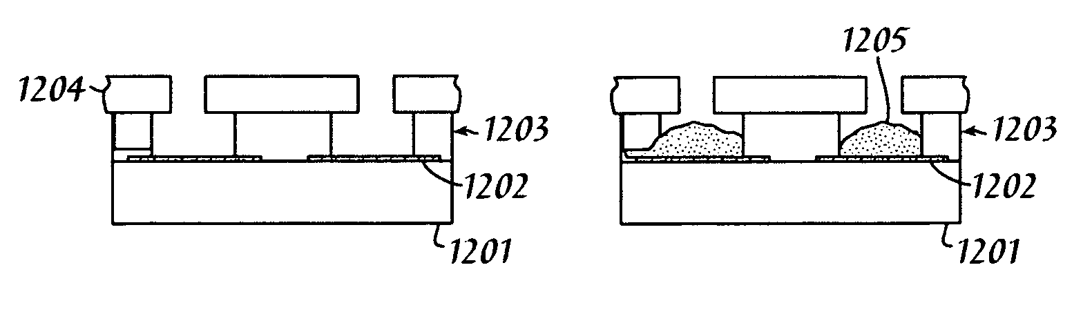
FIGS. The 12A-12C images show the placement and alignment on a cathode of a stencil 1204 mask. This cathode substrate is shown as having features like a cathode electrolyte layer 1202 or an insulating layer 1203. However, this process does not depend on the exact configuration as long as features in the stencil 1204 match the features of the cathode on which the CNT paste or ink 1205 is needed to be dispensed. The CNT paste or ink 1205 is printed using a screen-printing machine or other similar method through the stencil openings 1204.
To print on substrates 1201 that have a well structure as shown in FIG. The viscosity can be adjusted by using a stencil 1204 and an organic material (terpineol). The viscosity range of CNT ink is 8000 CP up to 100,000 CP. FIG. FIG. 12B illustrates that CNT ink can be dispensed through the stencil screen openings 1204 into the well structures. The thickness and size of the CNT paste or ink 1205 patch (FIG. The stencil mask openings 1204 are dispensed with CNT ink or paste 1205 (FIG. 12C. The thickness of CNT cathode 1205, or the patch, can be uniformly controlled by the self-flattening procedure. The uniformity of flatness is related to the uniformity in field emission images. The final thickness of CNT 1205 cathode may be as low as 2-15 m after firing until most of the solvent and organic binding materials are burnt away.
Advantages Of Stencil Screen
Using dispensing or Ink-Jet printing processes, a dispensing head is moved relative to the substrate. It then moves to the next location to deposit additional material. 3( a)). The following descriptions use a Musashi? In the following descriptions, a Musashi SHOT mini? Formulations may need to be adjusted depending on the type and model of dispenser. After the fluid CNT ink is placed into the well structure it can be covered completely by a wetting procedure (see FIG. 3( b)). The CNTs are still in the pixels after the ink, paste or drying has been completed (see FIG. 3( c)). Depending on the CNT material, this process can require UV (ultraviolet), heat, or both. CNTs will be contained within the well structure. The well structures can be made very accurately using techniques such as printing, dispensing or sandblasting. The process described above will produce uniform CNT deposition in each pixel if the well structures have been accurately made. Well structures can also be used to avoid edge emission problems that could also cause non-uniform performances. The well shape can determine the shape and the effective emitting area for a CNT pixel or subpixel.

To fill the wells evenly, it is important to prepare a uniform CNT ink or CNT paste and control the volume of ink or CNT paste in the hole. The CNTs conform to the wells by using different shapes, as shown in the FIGS. This is due to the hydrophilic and hydrophobic properties of the ink or paste of CNTs. 4(a) and (b). FIG. FIG. 5 shows a vacuum-sealed CNT-field emission display configured with the well-formation process as described in this invention. After the vacuum-sealed display has been evacuated, the sidewall spacers (wall spacers) and internal spacers maintain the gap between anode (phosphor screen), and cathode plates. According to the process(es), different CNT-based paints with excellent field emission properties were developed. The wells can be filled with CNT-ink using a dispenser, an inkjet, a screen printer and similar devices.
It is important to note, that no post-deposition process is performed after the CNT isk has been deposited in order to form a Cathode Structure. This includes the removal of any sacrificial layer, which may damage the CNT Ink. The U.S. Pat. discloses the importance of such sacrificial layer in its processes. No. 6,705,910. This damage will negatively affect the field emission capability of CNT ink.
Examples of suitable methods for filling CNT-ink in the wells of pixels include but are not limited, to dispensing (inkjet printing), screen-printing (spin-on coating), brushing or dipping and similar techniques.
The following examples are provided to illustrate the invention. They are not intended to limit the scope of this invention. Following are examples of CNT-ink formulations that can be used according to the process of the invention and the emission properties of each formulation.
Sample 1 (CNT-Ink 1):
The other components of composite were prepared in an inorganic material. The inorganic material, Resbond 989 (a mixture of Al2O3 and water with inorganic glues), was purchased from Cotronics Corp. in Brooklyn, N.Y. Composites containing other particles, such as sio2, can also be used. These particles can be semiconducting, insulating or conducting. Particle sizes can be smaller than 50 m. Resbond 989’s carrier is water. However, other materials can be used. They may be organic or inorganic. The composite may contain small amounts of other materials that enhance the properties of this material. These include binders, for example, alkali-silicates and phosphates.
Grinding of the Mixture
Click here to view the patent on Google Patents.