Invented by SONG; Byong Gwon, Kim; Jin Myoung, Park; Jae Chul, Yoon; Yong Seop, Lee; Du Hyun, Kim; Jae Kwan, Rhee; Choong Ho, SAMSUNG ELECTRONICS CO., LTD.


Thermal image sensors help us see what our eyes cannot. They turn invisible heat into clear pictures, guiding everything from night vision cameras to smart home security. Today, a new patent shows a smarter way to make these sensors—making them work better, use less power, and be easier to build. This article explains what this invention does, why it matters, and how it changes the game.
Background and Market Context
Thermal imaging is all around us. Security cameras, firefighting gear, drones, and even some cars use it to see in the dark or spot heat leaks. These sensors pick up infrared light, which is really just heat, and turn it into an image. Over the last few years, more products want to use thermal imaging because it keeps getting cheaper and smaller. But there’s just one big problem: making great sensors is still pretty hard.
For most of history, good thermal sensors needed to be cooled down to very low temperatures. This made them expensive and bulky. Then, “uncooled” sensors arrived. They work at room temperature, which made them easier to use in all sorts of gadgets. But even these uncooled sensors have limits. They can be tricky to make, may not be sensitive enough, or might use too much power for battery-powered things like drones or smart cameras.
Today, the market asks for sensors that are small, very sensitive, and cheap to make. Cameras want more pixels for clearer images. Smart homes want sensors that sip power but never miss a detail. Medical tools want safe, fast readings. This means inventors need to find new ways to build sensors so they can be tiny, smart, and ready for everything from doorbells to satellites.
This new patent, coming from research in Korea, is about solving these problems. The inventors looked at the way current sensors are built and found ways to make them even better. Their invention uses thin layers, clever wiring, and smart materials so that the sensors can pick up tiny temperature changes with less noise and less power. And, very importantly, it can be made using steps that fit right into how modern chips are already built. That means it could be scaled up for millions of devices.
In short, this patent aims to give the world thermal sensors that are easier to make, more sensitive, and ready for the next wave of smart products.

Scientific Rationale and Prior Art
To understand why this invention matters, let’s look at how today’s thermal image sensors work and what holds them back.
The most common type of uncooled sensors are called microbolometers. Each pixel in a microbolometer absorbs heat from incoming infrared light. When it warms up, its electrical resistance changes. By reading those changes, the sensor creates a picture of the heat in the scene.
The two most widely used materials in these sensors are vanadium oxide (VOx) and amorphous silicon (a-Si). Both are good at changing resistance when they get warmer. VOx sensors have been around a long time. They are sensitive but not always easy to make with modern chip processes. a-Si sensors work better with today’s chip factories, but sometimes they are less sensitive.
A key number for these sensors is “responsivity.” This is how much the sensor’s output changes for a given amount of heat. If the sensor is very responsive, it can see small temperature differences—which is great for sharp, clear images.
Responsivity depends on things like the material’s temperature coefficient (how much its resistance changes with heat), the amount of current running through it, and the design of the sensor. If you make the sensor thinner, it heats up faster but can also become noisy or fragile. If you make it thicker, it may not respond as quickly to heat changes.
People have tried many tricks to make sensors better. Some change the shape of the electrodes that pick up the signal. Others try to adjust the distance between the electrodes, hoping to get a cleaner current path. Some tried to shrink the support arms that hold the sensor above the chip, so less heat leaks away. But making the parts smaller can make the sensor harder to build and less stable.


When sensor makers try to pack more and more pixels into a small area (for higher resolution), the challenge grows. Smaller pixels mean less space for each sensor part, and heat can leak away faster, making it harder to see small temperature differences.
Another problem is that current designs don’t always use the energy from incoming light very efficiently. Some of the heat escapes before it can be measured, or the materials used are not perfect at absorbing the right wavelengths.
Finally, the way sensors are made today often involves many steps that don’t fit easily into the way modern computer chips are built. That means higher costs and more chances for problems in mass production.
This is the backdrop for the invention described in this patent. The inventors looked for ways to boost sensitivity, lower power use, and make the sensor friendly for large-scale chip manufacturing. Their solution is a new layout for the parts, new materials in key places, and a clever way of wiring things so that the sensor responds more strongly to small temperature shifts.
Invention Description and Key Innovations
This patent introduces a new design for a thermal image sensor—one that is both simple and powerful. The heart of the invention is a stack of very thin layers, suspended above a chip. Each layer has a special job, and together they work like a finely tuned instrument for detecting heat.
Let’s walk through how this new sensor is built and why each part matters.

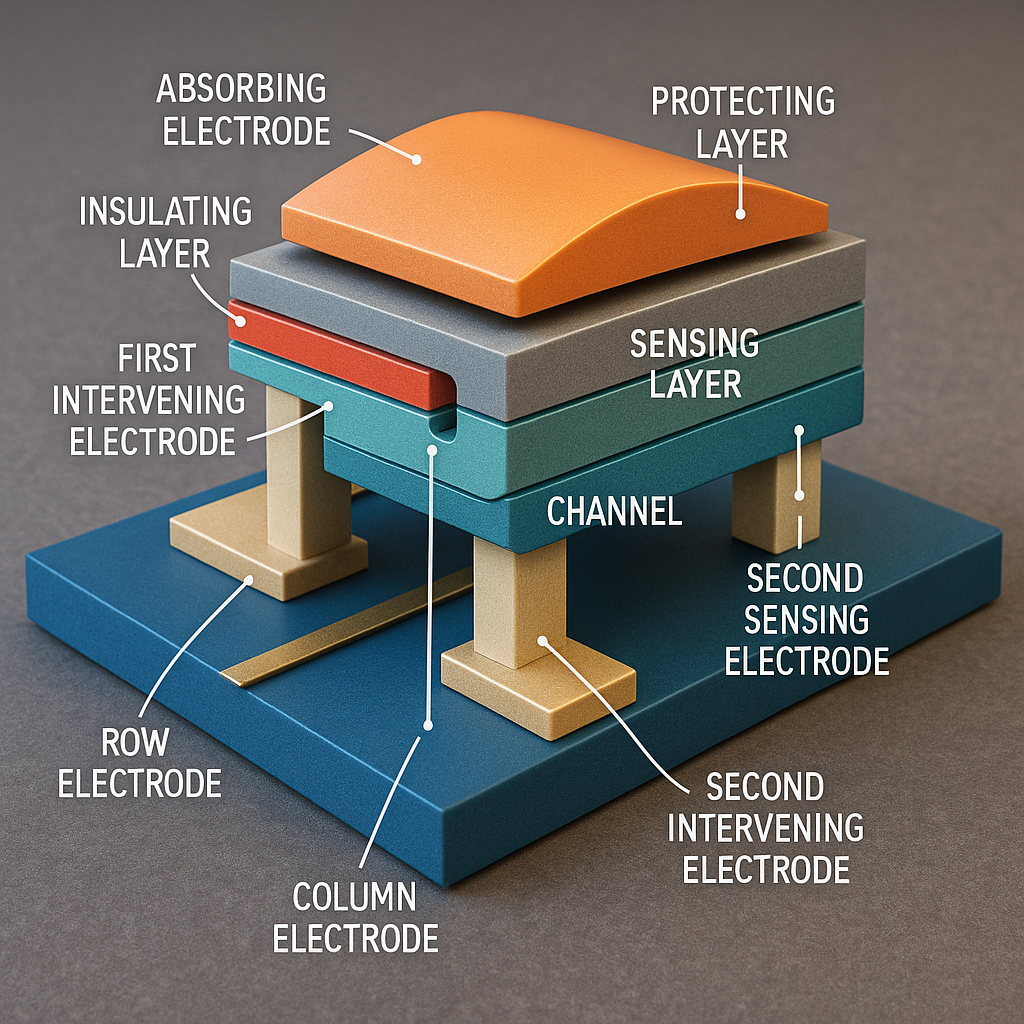
At the bottom is the substrate, which is just a fancy word for the base chip, often made from silicon. On top of this, the inventors lay down a grid of “row” and “column” electrodes. These act like the street grid for wiring up each pixel so the chip can read out the data.
Above the substrate, and separated from it by tiny support arms, is the multi-layer stack. This is where the magic happens. Here are the key layers:
1. The Sensing Layer: This thin film is made of amorphous silicon (a-Si). Its job is to soak up incoming infrared light and turn it into heat. When the layer gets warmer, its electrical resistance changes.
2. The Sensing Electrodes: Two small metal strips (made from titanium nitride, or TiN) touch the sensing layer. Between them is a “channel” where current can flow. When the sensing layer heats up, the current flowing between these electrodes changes—this is the signal that tells us what the sensor sees.
3. The Absorbing Electrode: This is a clever addition. It is also made from titanium nitride and connects to one of the sensing electrodes. Its job is to help absorb even more infrared light, boosting how much heat gets into the sensing layer. But it does something else, too: it creates an electric field (polarization) in the sensor, making it easier for current to flow even at low voltages. This means the sensor can work with less power, which is great for battery-powered devices.
4. The Insulating Layer: This thin film (like silicon nitride) separates the absorbing electrode from the other parts, making sure that electricity only flows where it’s supposed to. The design uses tiny holes (called via holes) to connect the right parts together without letting signals leak where they shouldn’t.
5. The Protecting Layer: This top layer covers everything up, keeping the parts safe from dust and damage.
The whole stack is held above the chip by special arms and legs. These supports are carefully designed so that heat does not leak away too quickly, letting the sensor pick up even tiny temperature changes.
One more smart addition is the resistance reducing layer. This is a thin extra layer between the sensing electrodes and the sensing layer. It’s doped with special chemicals (called donor or acceptor impurities) that make it easier for current to flow. This helps the sensor respond faster and with less noise.
The inventors also describe several ways to arrange these layers. For example, sometimes the absorbing electrode is above the sensing layer, sometimes it’s below. Sometimes the sensing electrodes are closer to the chip, sometimes further away. Each layout has pros and cons for different applications, and the patent covers all these options.
The manufacturing process is also new. The inventors describe step-by-step methods to build the sensor stack in a way that fits right into how modern chips are made. They use a “sacrificial layer” that gets removed at the end, leaving the stack floating over the chip. This process helps create the tiny gaps needed for sensitivity, and makes mass production much easier.
Because the materials used (like a-Si and TiN) are common in chip factories, this design can be ramped up for millions of sensors without needing new tools or expensive changes. The clever use of the absorbing electrode and resistance reducing layer means each pixel can operate at lower power, with stronger signals and less noise.
What does all this mean in practice? Sensors based on this patent can be made smaller, cheaper, and more sensitive than many current designs. They can pick up smaller temperature changes, which leads to clearer images. They use less power, so they’re perfect for battery-powered gadgets. And because the design fits with existing chip-making steps, they can be produced in big volumes for everything from smartphones to smart homes.
Conclusion
Thermal imaging is changing the way we see the world, from keeping us safe at night to powering the smart devices in our homes. The new patent described here points to a future where thermal image sensors are more sensitive, need less power, and are much simpler to make. By rethinking the way each part of the sensor is built and connected, this invention stands to bring better heat-sensing to more products, making our world smarter and safer. As new devices demand sharper vision and longer battery life, inventions like this one will help lead the way.
Click here https://ppubs.uspto.gov/pubwebapp/ and search 20250216266.