Invented by KIM; Junbae, LEE; Geunhee, SUNG; Yoochang, Samsung Electronics Co., Ltd.


In the fast-moving world of electronics, memory devices keep getting faster and smaller. But with higher speeds come new problems. One of the biggest is making sure that signals between memory chips and controllers stay clean and accurate. Today, we’ll break down a new patent that tackles this issue using a smart way to calibrate signal strength between stacked memory chips. If you’ve ever wondered how the latest memory sticks keep up with your computer’s speed, or how chip designers solve tricky problems, this article will walk you through everything, step by step.
Background and Market Context
Memory is at the heart of every computer, phone, and smart gadget. As we demand more speed and more power from our devices, the chips inside have to move information incredibly fast. This is especially true in data centers, gaming PCs, and servers, where every fraction of a second counts.
Over the past few years, manufacturers have stacked memory chips on top of each other to save space and boost performance. These are called multi-die memory devices. Instead of one big chip, you get many smaller chips (called “dies”) layered together. This makes memory smaller and faster, but also creates new challenges. When data moves quickly between these stacked chips and the memory controller, tiny changes in resistance (called “impedance”) can mess up the signals. If the impedance is not set just right, signals can get distorted or lost. This means your computer could slow down, crash, or make mistakes.
To fix this, memory makers use a process called impedance calibration. This process “tunes” the chips so signals are clear and strong. Traditionally, each chip would calibrate itself or rely on a central controller. But as chips get more complex and stacked closer together, this old way doesn’t always work well. When many chips try to calibrate at the same time, the signals can interfere with each other. The result is wasted power, more heat, and sometimes errors.

The market is hungry for solutions. Every big tech company wants memory that is faster, more reliable, and uses less energy. Cloud computing, AI, and high-end gaming all push the limits. That’s why this new patent matters. It introduces a new way for multiple memory chips to calibrate themselves—one after the other, in a smart order, without getting in each other’s way. This idea could help make future memory faster and more stable, giving users smoother experiences and letting manufacturers pack even more power into tiny spaces.
Scientific Rationale and Prior Art
Let’s take a step back and see why impedance calibration is so important. When a memory chip sends data to a controller, it does so by creating tiny electrical signals. These signals travel along wires, through connectors, and across the circuit board. For the signal to arrive cleanly, the resistance the signal sees (the “impedance”) has to match up between the chip and the board. If it doesn’t match, part of the signal bounces back, causing noise or even losing data. Think of it like echoes in a tunnel—if the tunnel isn’t shaped just right, your voice bounces back and you can’t hear clearly.
To solve this, chips use something called impedance calibration. This process tests the output circuits, adjusts some settings, and tunes the resistance until it matches what’s needed. Many memory chips use external resistors on the circuit board as a reference, so they can “know” what the right impedance should be.
Older methods let each chip or module calibrate itself when it powers up or when a special command is sent. However, as more chips are stacked together or placed close on the same board, their calibration steps can overlap. If they all try to talk to the calibration resistor at once, their signals can mix, causing errors. Some solutions tried to have each chip use a different wire or communication pad for calibration, but this adds complexity, takes up space, and can still cause interference.
Some previous inventions suggested using a master-slave relationship, where one chip (the “master”) calibrates first, then tells the others (the “slaves”) to go in turn. But even these methods often used extra wires, pads, or involved sending signals that could interfere with regular data movement or waste power.


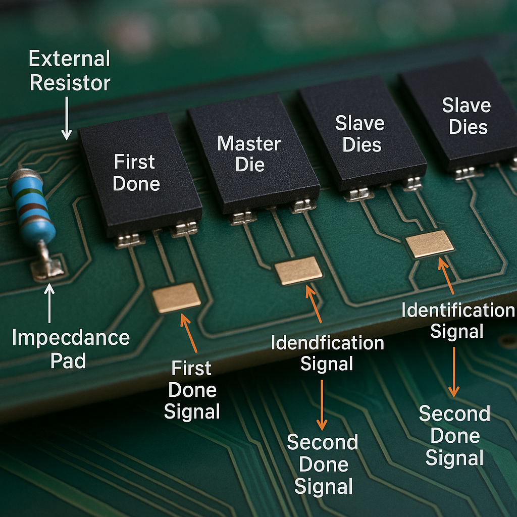
This patent builds on the master-slave idea but adds new features. It lets all the memory dies connect to the same calibration resistor using their own “impedance pads.” The master chip calibrates first, then signals the next chip to go, then the next, and so on. Each chip waits its turn, using smart logic to know when it’s time to calibrate. This makes the process orderly, avoids interference, and doesn’t need extra wires or complex connections. The chips talk to each other using the same pads they use for calibration, keeping the design simple and the board clean.
Another smart feature is that each slave chip uses a combination of signals and built-in “fuse” information to know exactly when it’s their turn. This fuse info is programmed at the factory so each chip knows its unique identity. As a result, calibration happens in the right order, every time, no matter how many chips are stacked.
Invention Description and Key Innovations
Now let’s break down how this invention actually works, using simple words.
Imagine a group of memory chips (dies) all sitting on the same board. One chip is picked to be the master. The rest are the slaves. All these chips share a connection to a calibration resistor on the board. This resistor acts like a “teacher” telling the chips what the correct impedance should be.
Here’s what happens step by step:

First, the master chip starts the calibration. It gets a command—either from the memory controller or from its own settings—and begins adjusting its output circuits. Its goal is to match its impedance and reference voltage perfectly to what the resistor expects. When it finishes, it sends a “done” signal out through its impedance pad, which is connected to the same resistor. This signal can be seen by all the slave chips.
Each slave chip has its own smart logic to watch for this “done” signal. But they don’t all jump in at once. Instead, each slave has a unique ID, set by special fuse bits programmed during manufacturing. These fuses act like a name tag. When a slave sees the “done” signal, it checks if it’s supposed to go next by comparing the signal with its own fuse info and a counting signal. If it’s the right time, that slave begins its own calibration, adjusting its output circuits to match the correct impedance and voltage. When done, it sends out its own “done” signal through its impedance pad.
The next slave sees this new “done” signal and checks if it’s their turn, and so on. This way, each chip calibrates one after another, never at the same time. It’s like students lining up to talk to the teacher one by one instead of all shouting at once. This orderly process keeps signals clean and avoids problems.
Inside each slave chip, several small circuits help make this work:
– A level shifter takes the incoming analog signal from the impedance pad and turns it into a digital signal the chip can understand.
– A ripple counter keeps track of calibration steps.
– A fuse set stores the unique ID for the chip.
– An identifier generator checks the fuse info and counting signal to decide when it’s that chip’s turn.
– The impedance calibration circuit does the actual tuning, adjusting the output driver to match the required impedance.
Once all chips have calibrated, the memory device is ready to run at high speed, with clear, strong signals between each chip and the controller.
This design can also run “background” calibrations during idle times. The master chip can start a new round of calibration when things are quiet, keeping everything in tune even as conditions like temperature or power change.
A big benefit of this design is that it works for both two-dimensional (chips placed side by side) and three-dimensional (chips stacked on top of each other) memory packages. It also works with different types of memory, like DDR and high-bandwidth memory (HBM), and can be used in all sorts of devices—from gaming PCs to servers to smartphones.
By having each chip calibrate in order, using shared connections and simple logic, this invention keeps the board tidy, reduces interference, and helps maintain strong, reliable signals even as memory speeds climb higher. For users, this means faster, more stable devices with fewer crashes and better battery life.
Conclusion
As computer memory evolves, keeping signal quality high becomes even more important. This new patent offers a clever, simple way for many memory chips to calibrate themselves, one after the other, using shared connections and smart logic. By letting the chips talk through the same impedance pads and using factory-set fuse information to organize the process, it avoids signal clashes and wasted energy. This means future devices can be faster, smaller, and more reliable, giving everyone from gamers to cloud users an even better experience. If you’re in the business of designing or using cutting-edge memory, this technology is a big step forward in making sure your data moves quickly and safely every time.
Click here https://ppubs.uspto.gov/pubwebapp/ and search 20250218478.