Invented by Arbore; Mark A.
Photonic integrated circuits (PICs) are changing the way we use and control light on a small chip. This new patent application introduces a fresh idea for designing these circuits. By using special curved lenses right on the chip, called asymmetric aspheric on-chip lenses, the inventors make it easier to shape and direct light beams in new ways. In this article, we’ll break down what this means for the market, how it builds on past science, and what’s really new and useful about this invention.
Background and Market Context
Light travels very fast and carries a lot of information. For years, scientists and engineers have worked to control light for things like the internet, sensors, and measuring tools. At the heart of these systems are photonic integrated circuits, or PICs. These are tiny chips that handle light, much like computer chips handle electricity.
Today, many devices—from data centers to medical scanners—need to move and shape light in very precise ways. These devices often have to be small, reliable, and cheap. Photonic integrated circuits help achieve this, but there are still challenges. For example, when light exits a chip, it often spreads out or bounces back, which can cause problems. Sometimes, extra pieces like lenses or mirrors must be added, making the system bigger and more complex.
The need for smaller, smarter, and more flexible optical systems keeps growing. In fields like telecommunications, companies want to squeeze more data through smaller cables. In medicine, scientists want to measure tiny changes in the body using light. In factories, machines use lasers to check the quality of products. All these uses need better ways to generate, guide, and shape light on small chips.
This is where the new patent comes in. It focuses on ways to build special lenses right onto the edges of photonic integrated circuits. These lenses aren’t just simple curves—they have shapes that can change how light spreads and how intense it is across the beam. With these lenses, light can be shaped more exactly before it even leaves the chip. This can make systems simpler, smaller, and more powerful.
As companies look for easier ways to design optical systems, inventions like these are important. They give designers more control right on the chip, which could lower costs and open up new possibilities in all kinds of industries.
Scientific Rationale and Prior Art
To understand why this invention matters, it helps to look at how light is usually handled on photonic chips and what has been tried before.
Most photonic chips use waveguides. These are tiny paths that guide light, much like wires guide electricity. When light needs to leave the chip, it often goes through a flat surface called a facet. But when light hits this flat edge, some of it bounces back into the chip. This can cause interference and mess up the light source. Sometimes, extra lenses are used outside the chip to shape the beam, but these add size and cost.
Some earlier inventions tried to solve this by curving the chip’s edge into a simple shape, like a half-circle. This can help focus the light and reduce some of the problems. For example, some patents describe making a small lens right on the chip by shaping its side. This lens focuses the light as it leaves the chip, helping get more light out in the right direction.
But these earlier lenses usually have a simple, even curve. When light passes through them, the beam keeps its original intensity shape, often called a Gaussian profile. In a Gaussian beam, the light is brightest in the middle and fades toward the edges. Sometimes, though, it’s better to have a beam where the light is spread out more evenly, like a flat-top shape. This is especially true if you want to light up a whole area evenly or measure something with consistent brightness.
Changing the beam shape after it leaves the chip is possible, but it usually means adding more lenses or diffusers. These extra parts can make the system bulky and harder to align. Also, making sure that light doesn’t bounce back into the chip (back-reflection) is tricky, especially when using outside lenses.
Some research has looked at tilting the waveguides or offsetting them, so that any light that bounces back from the chip’s edge doesn’t go straight back into the waveguide. This helps, but doesn’t solve the problem of shaping the beam’s intensity.
What has been missing is a simple way to shape the outgoing beam’s intensity right on the chip, while also controlling the angle and reducing back-reflection. The new invention addresses this by making the on-chip lens not just curved, but also asymmetric (not the same on both sides) and aspheric (not a simple circle). This new shape gives much more control over how the light spreads and where it goes.
In summary, while the building blocks—waveguides, slab regions, and simple on-chip lenses—have been used before, this patent brings new ideas in how these pieces work together to solve real problems in shaping light on a chip.
Invention Description and Key Innovations
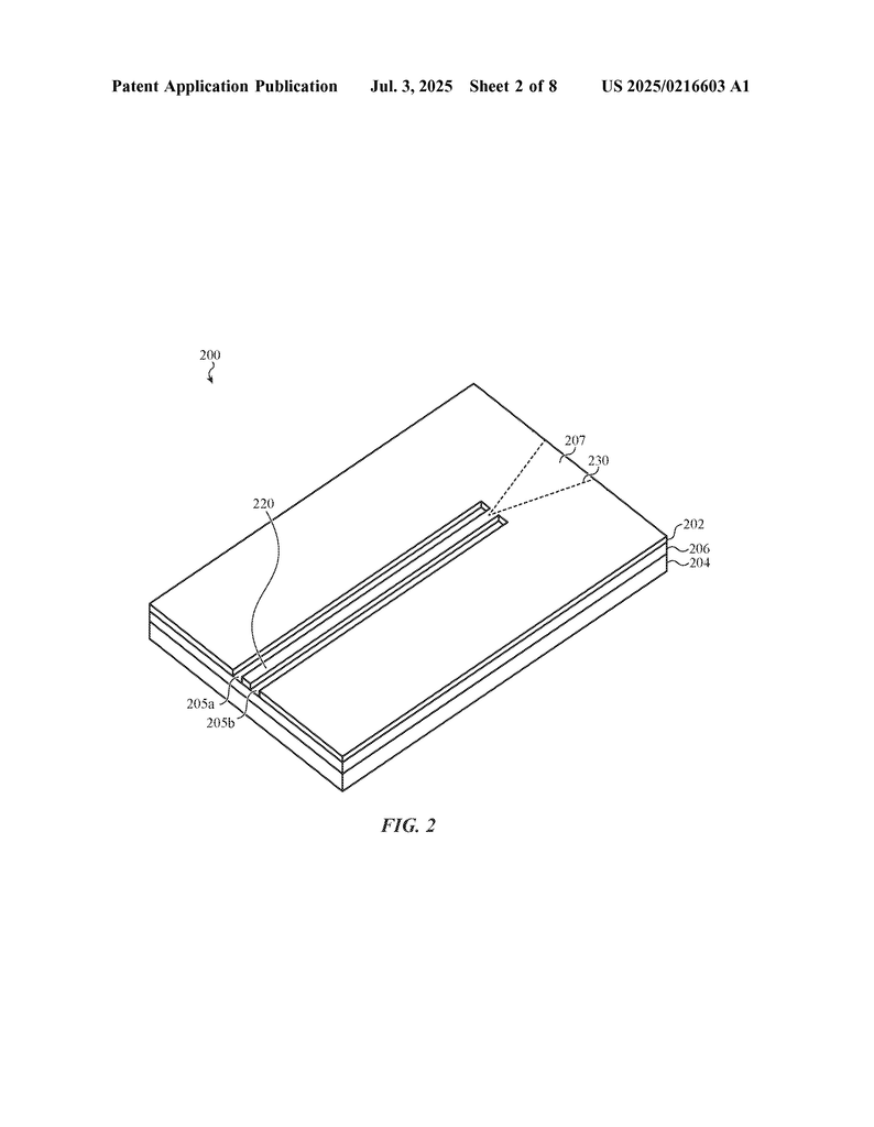
This patent application introduces a photonic integrated circuit with a special kind of on-chip lens. The lens is built right into the edge of the chip, using the side surface of the slab waveguide. But, unlike past designs, this lens has an asymmetric and aspheric curve. That means it’s not just a regular arc or circle. Its shape changes across the lens, giving more control over the light that passes through it.
Let’s break down the main parts and what makes them special:
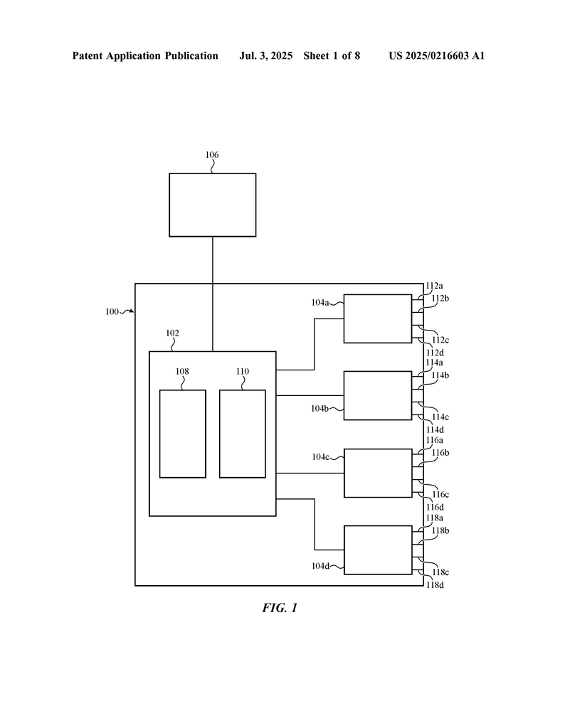
First, the chip has a waveguide layer. This includes a regular waveguide, which brings the light, and a slab waveguide, which spreads the light out. The waveguide ends at the slab, and the slab leads to the edge of the chip, where the on-chip lens is formed.
The on-chip lens is not just a simple curve. It has an intermediate area in the middle with a larger radius of curvature (making it less curved), and two side areas (peripheral portions) with a smaller radius (more tightly curved). When the light beam comes in, the center of the beam goes through the less curved middle, while the edges go through the more curved sides.
This shape changes the way the light spreads as it leaves the chip. The more curved sides focus the light more, making the beam brighter at the edges than it would be with a normal lens. This helps flatten the intensity profile across the beam—so the brightness is more even from one side to the other. It’s a simple way to get a flatter, more useful light beam without extra parts.
Another key idea is the way the waveguide is positioned. Instead of being straight on, the waveguide is tilted compared to the direction of the output beam. This tilt can be nine degrees, twelve degrees, or more. By choosing the right angle, any light that bounces back from the lens doesn’t go straight back into the waveguide. This helps keep the light source stable and avoids unwanted feedback.
This design can be used for just one emitter, or for many emitters on the same chip. Each emitter can have its own lens shape and tilt angle. This means you can design different emitters to make beams that point in different directions or have different intensity profiles. The beams from these emitters can overlap to form a bigger composite beam, which can then be further shaped or diffused as needed.
You don’t have to make all the lenses the same. Some can have different curves, so each beam can be tailored for a specific job. For example, in a measuring device, you might want one beam to be very even, while another is focused more tightly. The controller on the chip can turn each emitter on or off, or change the light’s wavelength, giving lots of flexibility.
By flattening the beam’s intensity right on the chip, designers can use simpler, smaller outside optics. This can make the whole system smaller and easier to build. Also, because the chip can direct beams in different angles, it’s easier to combine them or shape them for special uses.
In summary, the key innovations are:
– The on-chip lens has an asymmetric, aspheric shape to flatten the output beam’s intensity.
– The waveguide is tilted to prevent back-reflection into the light source.
– Each emitter on the chip can have its own lens shape and tilt angle.
– Multiple beams can be combined to make a larger, more useful output.
– This all happens right on the chip, with fewer outside parts needed.
These new ideas make it easier to design optical systems that are smaller, simpler, and more flexible—meeting the growing demands of modern technology.
Conclusion
Photonic integrated circuits are a big part of our future, helping us use light in new ways for communication, measurement, and more. This new patent application shows a creative leap, using curved lenses built right onto the chip to shape light beams more exactly. By flattening the beam’s intensity and controlling its direction, all on the chip, this design solves real problems faced by engineers and opens up new possibilities for optical systems. Whether in data centers, medical tools, or factory sensors, this approach could make devices smaller, cheaper, and more powerful. As technology moves forward, inventions like these will help light do even more for us, in ways that are easier to use and understand.
Click here https://ppubs.uspto.gov/pubwebapp/ and search 20250216603.


