Invented by Sandhu; Gurtej S.
### Self-Assembled Nucleic Acid Nanostructures: A New Frontier in Nanofabrication
#### Introduction: Redefining Nanostructure Fabrication
The relentless trend towards miniaturization shapes the future of electronics, materials science, and biotechnology. At the heart of this movement is the challenge of reliably creating features at the nanoscale—below 50 nanometers (nm)—with both precision and scalability. Conventional photolithography, the workhorse of microfabrication, is encountering fundamental physical and economic barriers as features approach these minuscule dimensions.
Enter self-assembled nucleic acids—a class of programmable biopolymers capable of forming intricate, nanometer-scale patterns on a variety of substrates. The patent family described above introduces groundbreaking methods that not only leverage the self-assembly properties of nucleic acids like DNA and RNA for nanofabrication, but also overcome significant reliability challenges by incorporating biochemical repair mechanisms. The net result is a method for forming low-defect, highly precise nanostructures on substrates such as silicon, metals, and polymers, with critical dimensions less than 50 nm. This blog will walk you through the science, potential applications, and market prospects for this technology.
—
#### Restating the Invention: From Biomolecules to Defect-Free Nanopatterns
At its core, the patented method includes the following steps:
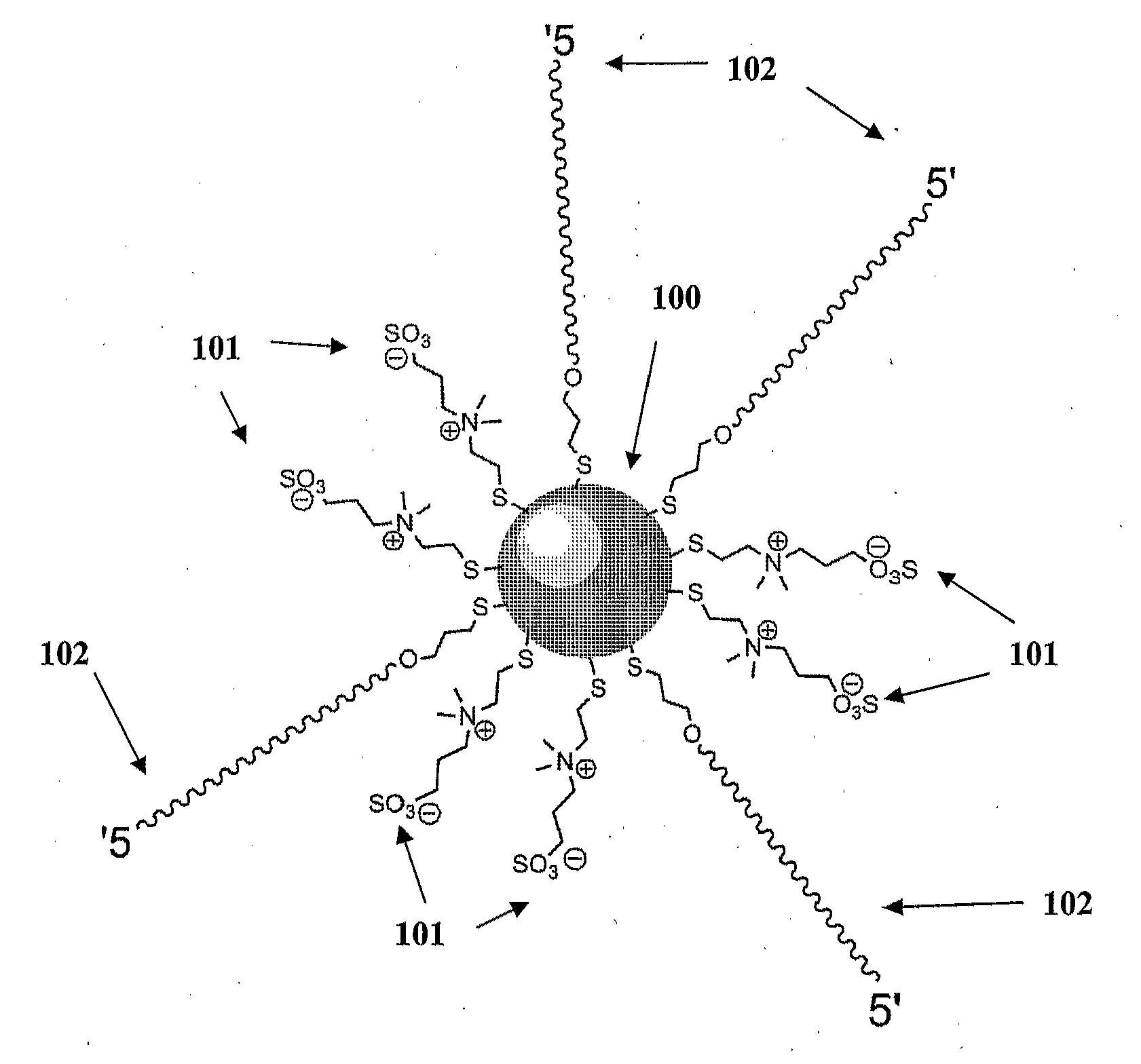
1. **Design and Synthesis**: Specific nucleic acid sequences are computer-designed to self-assemble into predetermined nanostructures.
2. **Self-Assembly and Patterning**: When dissolved in solution and deposited onto a substrate (e.g., via dipping, spraying, or coating), these sequences spontaneously organize through complementary base pairing. The result is an initial nanopattern on the substrate—potentially comprising multi-stranded complexes, scaffolded structures, or single long strands.
3. **Defect Identification and Repair**: Inevitably, the self-assembled structure will exhibit defects—mispaired bases, incomplete folding, or gaps. Advanced metrology techniques (optical or e-beam) can identify these defects.
4. **Enzyme-Mediated Repair**: The deposited pattern is exposed to one or more DNA/RNA repair enzymes, carefully selected based on the nature of defects present. These enzymes catalyze correction steps, such as base excision or heterocycle formation, significantly lowering the defect density.
5. **Pattern Transfer to Substrate**: The corrected nucleic acid pattern serves as a high-resolution mask or template for transferring intricate features onto the substrate, using etching or deposition techniques.
6. **Removal and Further Processing**: The nucleic acids and any sacrificial layers are subsequently removed, revealing a nanostructured substrate suitable for further device fabrication (e.g., semiconducting nanowires, metal nanoparticles, quantum dots).
This methodology enables the fabrication of dense, patterned nanostructures with critical dimensions well below the limits of conventional photolithography and block copolymer self-assembly—while substantially improving yield and process reliability.
—
#### Potential Applications of Low-Defect Nucleic Acid Nanopatterning
The applications for such a versatile, high-precision nanofabrication platform are vast and transformative. Key areas are:
##### 1. **Semiconductor Devices and Integrated Circuits**
Shrinking CMOS (Complementary Metal-Oxide-Semiconductor) transistor sizes below 5 nm is pushing traditional lithographic techniques to their limits. DNA/RNA-based patterning:
– Allows creation of sub-20 nm features: transistors, nanowires, and interconnects.
– Can serve as a replacement or complement to extreme ultraviolet (EUV) or e-beam lithography.
– Reduces cost and complexity in next-generation memory, logic, and photonic chips.
##### 2. **Quantum Computing and Single-Electron Devices**
Reliable fabrication of quantum dots, single-electron transistors, and other quantum-scale devices demands atomic-scale patterning. Self-assembled nucleic acid templates:
– Provide accurate arrays for quantum dot localization.
– Enable integration of single-atom features needed for solid-state quantum processors.
##### 3. **Nano-Biointerfaces and Biosensors**
Surface patterning at the nanoscale is critical for biosensing, DNA sequencing chips, and lab-on-a-chip devices:
– Allows arrangement of capture probes, antennas, or reaction chambers below 50 nm.
– Supports multiplexed sensing with ultra-high spatial resolution.
##### 4. **Photonic and Metamaterials**
Control of nanoscale features determines the photonic bandgap and optical properties of materials:
– Enables the production of photonic crystals and metamaterials with tailored electromagnetic responses.
– Facilitates plasmonic design for quantum optics and energy harvesting.
##### 5. **Flexible Electronics and Wearables**
Patterning on flexible substrates (polymers, plastics) is notoriously difficult at sub-50 nm scale. This approach:
– Supports low-temperature, solution-based processing.
– Can be adapted for roll-to-roll manufacturing of flexible displays, sensors, and transparent conductors.
##### 6. **Nanomedicine and Drug Delivery**
Nanoscale features on carrier surfaces influence biodistribution, cell uptake, and therapeutic efficacy:
– Patterned substrates can direct cell growth, differentiation, or tissue regeneration.
– Nano-arrays can control the spatial presentation of ligands or drugs.
—
#### Market Size: Total Addressable Market (TAM)/Serviceable Available Market (SAM)
Quantifying the commercial opportunities for such a multidisciplinary technology requires examining several overlapping markets:
##### **A. Semiconductor Manufacturing**
– **TAM**: According to SEMI and IC Insights, the global semiconductor fabrication equipment market is forecast to exceed **$100 billion (USD) in 2024**. The total semiconductor market (chips, devices, foundry services) is projected at nearly **$600 billion**.
– **SAM (Nanolithography & Process Materials)**: Emerging lithographic techniques—EUV, e-beam, maskless, and alternative patterning—currently occupy about **$5–$10 billion** in annual expenditures. Adoption of new self-assembly-based lithography could plausibly capture **5–10%** of this segment within 10 years: **$500 million to $1 billion** per year.


##### **B. Advanced Biosensing and Biochips**
– **TAM**: The global biosensors market exceeded **$30 billion** in 2022 and is rapidly growing, outpacing 8% CAGR mainly due to medical diagnostics, environmental monitoring, and food safety sectors.
– **SAM (Nanoscale Biosensor Platforms)**: Nanoscale patterning methods impact platforms such as DNA sequencing, protein microarrays, and lab-on-chip devices—representing at least **$3–$5 billion** annually.
##### **C. Quantum Computing Hardware**
– **TAM**: The quantum computing market is nascent but expanding; hardware spend is expected to cross **$5–$10 billion** annually by 2030.
– **SAM**: Companies such as IBM, Google, and Intel are actively seeking advanced nanofabrication methods for quantum dots, Josephson junctions, and atomic arrays—potential addressable market for this technology could conservatively be **$500 million–$1 billion** per year within the next decade.
##### **D. Photonic/Metamaterial Devices and Flexible Electronics**
– **TAM**: The global photonics market (sensors, optical circuits, communications) is projected at **$750 billion by 2030**.
– **SAM (Nanoscale Photonics/Metamaterials)**: Nanoscale patterning is particularly critical for next-gen sensors and displays; the relevant annual spend could be **$1–$2 billion**.
##### **Summary Table**
| Application | TAM (USD, 2024+) | SAM (USD, Potential Share) |
|—————————–|——————|————————————–|
| Semiconductor Lithography | $100B+ | $500M–$1B |
| Biosensors/Biochips | $30B+ | $3–$5B |
| Quantum Computing Hardware | $5–$10B (2030) | $500M–$1B |
| Photonics/Metamaterials | $750B (2030) | $1–$2B |
| Flexible Electronics | $40B+ | $1B (overlap with above) |
*Note: TAM and SAM estimates are cross-referenced from SEMI, IC Insights, Yole Developpement, BCC Research, MarketsandMarkets, and Omdia reports as of late 2023/early 2024.*
—
#### Competitive Advantages and Innovation Value
Why does this nucleic-acid-based methodology represent a leap forward, rather than incremental progress?
1. **Beyond Photolithography**: The method breaks free from the limits of optics; feature size is dictated by the molecular design, not the wavelength of light.
2. **Error Correction by Design**: The use of biologically-inspired repair enzymes enables post-assembly defect correction—a unique advantage vs. purely chemical or physical self-assembly that lacks dynamic repair.
3. **Programmability and Flexibility**: Virtually any pattern can be encoded into the nucleic acid sequence and folded to specification, unlocking rapid prototyping of custom devices.
4. **Material Versatility**: Process compatibility with glass, metals, polymers, and semiconductor substrates supports heterogeneous integration, crucial for next-gen integrated devices and sensors.
5. **Lower Energy and CapEx Requirements**: Solution-based processing and the avoidance of high-cost photomasks or e-beam writers reduce both energy use and equipment investment.
These advantages have broad appeal for industries seeking ever-smaller, more functional, and less costly components—from consumer tech to medical diagnostics to aerospace.
—
#### Challenges and Considerations
No transformative technology is free from challenges, and stakeholders must be mindful of the following issues:
– **Large-Scale Manufacturing**: While self-assembly is inherently parallel and scalable, uniform defect repair and pattern transfer at wafer scale (300 mm or beyond) must be rigorously demonstrated.
– **Stability and Process Integration**: Nucleic acids are susceptible to physical and chemical degradation; process conditions (e.g., solvents, temperature) must be designed to preserve pattern integrity until mask removal.
– **Enzyme Reproducibility and Cost**: Industrially scalable production of highly active, stable repair enzymes (potentially via recombinant methods) is a prerequisite for cost-effective adoption.
– **IP and Regulatory Landscape**: Regulatory frameworks (e.g., REACH, RoHS) regarding the use of biopolymers and enzymes in manufacturing should be analyzed, though most enzyme/nucleic acid materials have a favorable profile.
—
#### Conclusion: A Platform Technology for the Post-Lithography Era
The disclosed method of fabricating nanostructures using defect-repaired, self-assembled nucleic acid patterns is poised to alter the landscape of nanomanufacturing. The ability to pattern features below 50 nm, with improved reproducibility and functional complexity, opens pathways in semiconductors, quantum computing, biointerfaces, and beyond.
Given current and projected market sizes, as well as the demand for ever-smaller and more complex nanostructures, the commercial potential for this platform is substantial—potentially amounting to billions of dollars per annum as adoption spreads. Moreover, the modular, programmable, and error-correctable nature of the technology puts it at the forefront of the transition from traditional top-down to hybrid bottom-up/top-down nanofabrication.
For IP holders, startup founders, investors, and R&D leaders, this technology is not just a step towards the future—it is an enabler of new product paradigms, devices, and industries. The era of biomolecular nanolithography, once theoretical, is now on the cusp of commercial reality.
—
#### About the Author
*The author is a US-licensed patent attorney with expertise in nanofabrication, life sciences, and deep tech IP strategy. This article is intended for informational purposes and does not constitute legal advice.*
—
#### References
1. SEMI Industry Forecast, 2024
2. MarketsandMarkets: Biosensors & Biochips Market, 2023–2028
3. Yole Developpement: Lithography Equipment Market, 2023
4. BCC Research: Photonic Materials and Metamaterials, 2024
5. Omdia: Quantum Computing Hardware Market Trends, 2023
—
**Contact us** for further analysis, IP portfolio review, or licensing opportunities related to nucleic acid nanolithography!
Click here and search US 20250166993 A1.