Invented by Shan; Bohan, Pietambaram; Srinivas, Waimin Almendares; Jose Fernando, Carrazzone; Ryan Joseph, Arrington; Kyle Jordan, Lin; Ziyin, Chen; Haobo, Xu; Dingying, Feng; Hongxia, Duan; Gang, Guo; Xiaoying


In today’s electronics, we want everything to be smaller, faster, and more reliable. The way we put together tiny chips inside our phones, computers, and gadgets is always changing. One of the latest ideas is to put semiconductor chips inside a glass core. This new way could make our devices work better. Let’s explore why this is important, what has been done before, and what makes this new invention stand out.
Background and Market Context
Electronics keep getting smaller and more powerful. Think of your phone, your laptop, or even your smart refrigerator. All these devices need little chips, called integrated circuits (ICs), to make them run. These chips are made from silicon and need to connect to the rest of the device. To connect the chip to the main board (like a motherboard), companies use something called a package substrate. This is like a bridge between the chip and the big board.
Old package substrates were often made from organic materials or even ceramics. While these worked, they had limits. As chips got smaller and faster, these old materials could not keep up. They might bend, break, or even mess up the signals inside the device. This is a big problem because even a tiny mistake can make a device slow or cause it to stop working.
Another big challenge is that chips need help getting power. They need things like capacitors and voltage regulators nearby to make sure they get the right amount of energy. In the past, these helpers were placed on the outside of the package, taking up space and adding little bumps that can get in the way.
The market needs a new way to package chips. The goal is to make things smaller, more reliable, and better at handling power. This is where glass cores come in. Glass is strong, stable, and does not bend easily. It can handle heat and does not change shape much. Using glass as the main “core” of the package substrate could solve many problems.
But putting chips inside glass isn’t easy. The chip and the glass are made in very different ways. Chips are thin and fragile, while glass can be much thicker. If you just stick a thin chip into a thick piece of glass, the chip might move or not fit well. If the chip is not lined up just right, it won’t connect the way it should, making the whole device fail. So, the market wants a way to put these chips in glass, keep them safe, and make sure they line up just right.
This is not just a technical problem; it’s also about money. If you can package chips better, you can fit more features into smaller devices. You use less material, save space, and make products that last longer. Companies that make smartphones, computers, and even cars are all looking for the next big thing in chip packaging. Everyone wants their product to be faster and more reliable than the competition. Embedding chips into glass cores could be that next step.

Scientific Rationale and Prior Art
Let’s talk more about the science behind this. When you look inside a chip package, you see layers and connections. Each layer has a job. Some layers carry power, some carry signals, and others protect the chip. The core of the package is like the backbone of the whole thing.
In the past, the core was often made of an organic material, like a plastic with glass fibers. These are called “prepreg” cores. They are light and cheap but can bend and twist when things get hot or cold. This bending can break the tiny wires or connections inside, leading to device failures. Sometimes, ceramic cores were used. These are strong and stable but can be expensive and hard to work with.
Glass is different. It’s very stable and does not change much with temperature. It’s also very flat, which is good when you want to line up tiny chips. Glass does not have little fibers inside that can move around or cause weak spots. But there are challenges. Glass is hard to cut and shape. Making little holes, called vias, through glass is tricky. You need to use lasers or special chemicals to make the holes without breaking the glass.
Earlier inventions tried to solve the problem in different ways. Some tried to embed chips in plastic, but the chips could still move around during manufacturing. Others tried to glue chips onto the surface of glass, but then you don’t get the benefit of putting the chip inside the glass where it’s more protected.
Another problem is the size mismatch. Chips made by wafer processing are only so thick—usually less than 800 micrometers. Glass cores can be much thicker, maybe even two times as thick. If you try to fill the gap with glue or some filler, the chip might float, tilt, or move while the glue dries. This can cause the chip’s contact pads to be out of line with the rest of the package, leading to bad connections.
Some earlier inventions tried to use little steps or platforms inside the cavity where the chip sits. This helps to hold the chip in the right place. But making these steps in glass is not easy. You need to use careful laser etching or wet etching (using chemicals) to make the surfaces just right. If the step is too deep or too shallow, the chip won’t sit flush with the surface, and you’ll get the same problem as before.
Other attempts used just a simple hole in the glass, then filled up the gap with lots of glue. But too much glue can cause problems later. When the glue dries, it can pull on the chip or glass, causing warping or stress. This can make the whole package bend or crack. Also, glue and glass expand and contract at different rates when they get hot or cold, so over time, the chip might move or the package might break.


There is also the issue of making electrical connections through the glass. To get signals and power from the chip out to the rest of the device, you need to run metal lines through the glass. These are called “through glass vias” or TGVs. Making TGVs is hard because glass does not conduct electricity, and you need to fill the holes with metal without leaving gaps or cracks.
In summary, old ways of putting chips into substrates had many problems:
– Chips could move or not line up.
– Too much glue could cause stress and warping.
– Hard to make holes in glass for electrical connections.
– Hard to keep everything flat and in the right place.
This is why there’s a need for a new method—one that lets you put a chip into a glass core, hold it steady, keep it flat, and make all the right connections, all while using less glue and making the process reliable and repeatable.
Invention Description and Key Innovations
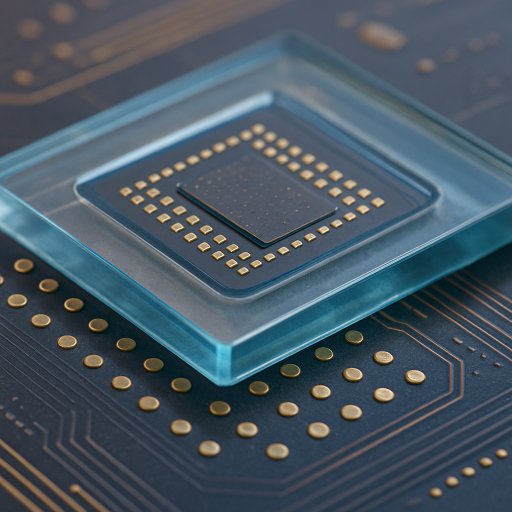
Now, let’s look at how this new invention solves all these problems. The main idea is simple: make a special cavity in a glass core, put a chip or capacitor inside, and make sure the top of the chip is exactly level with the surface of the glass. This sounds easy, but it takes some clever tricks to make it work.
First, the glass core is made with a cavity—like a little pocket—on one side. The surface of the glass is very flat, and the cavity is made using lasers or chemicals to be just the right depth and shape. In some cases, there is even a step or platform inside the cavity, so the chip has a flat spot to sit on. This step is made to match the thickness of the chip, so when the chip is placed inside, its top is flush (level) with the top of the glass. This is important because it means the chip can connect to other layers above it without any gaps or bumps.
Sometimes, the cavity has slanted walls or special ridges. These help guide the chip into place and stop it from moving sideways or tilting. The walls might be at different angles to help the chip “slide” into the right spot. In some versions, there are even multiple steps inside the cavity, so you can put the chip deeper or shallower, depending on its size.

To hold the chip in place, glue or adhesive is used. But unlike old methods, you don’t need to use a lot of glue. The chip sits on the step, and just a thin layer of adhesive goes underneath or around the sides. This keeps the chip steady while the glue dries. Sometimes, a special film called “die attach film” (DAF) is used instead of liquid glue. This film is stuck to the bottom of the chip and then pressed onto the step inside the cavity.
To get power and signals into and out of the chip, holes (vias) are made through the glass from the bottom of the cavity to the other side of the glass core. These vias are filled with metal to make them conduct electricity. In some designs, glue is also put inside the via, going up from the bottom to help bond the chip to the glass and keep everything strong.
The real innovation here is how everything lines up. When the chip is placed in the cavity, its top surface is in the same plane as the surface of the glass. That means connectors or pads on the chip are level with the glass surface, making it easy to connect to the next layer. This is called being “coplanar.” Coplanarity is very important in chip packaging because even a tiny misalignment can cause connection failures.
The invention also allows for different shapes and angles inside the cavity. This means it can handle chips or capacitors of different sizes. It can even have more than one cavity, or a cavity inside a cavity, to hold more than one chip or to position a chip even more precisely.
Here’s how the process works in simple terms:
1. Make a cavity in a piece of glass. The cavity has a step or platform inside.
2. Make a hole (via) through the glass from the cavity to the other side, if needed.
3. Put a thin layer of glue or a glue film on the platform or on the bottom of the chip.
4. Place the chip inside the cavity, so it sits on the step. The top of the chip is flush with the glass surface.
5. Fill the via with glue and/or metal to hold the chip in place and make electrical connections.
6. The chip is now safely embedded inside the glass, with its contact pads level with the surface.
This method solves the problems of the past:
– The chip cannot move, tilt, or float, because it sits on a solid step.
– Only a small amount of glue is needed, so there is less warping or stress.
– The chip and the glass are always at the same level, so connections are reliable.
– Making holes for electrical connections is easier because the process is planned from the start.
The invention also allows for creative shapes inside the cavity. The walls can be slanted or stepped, or there can be ridges or chamfers. These features help guide the chip into place and hold it steady during manufacturing. The steps and walls are made by careful etching or laser work, so they are very precise.
This method can work for many types of chips, not just standard ones. It can hold capacitors, which are used to store energy and help regulate power in the device. Having a capacitor close to the main chip helps the device run smoother and more efficiently.
Another key point is flexibility. The invention can be used with or without the through-glass via, depending on what kind of chip or device is being packaged. It can use liquid glue or a glue film, depending on what works best for the device.
Because the chip is level with the glass, you can build more layers on top, or connect it to other chips in a stack. This makes it easy to design multi-chip packages or add more features in the same space.
In the end, this invention is about making chip packaging better. It makes devices smaller, more reliable, and easier to build. It reduces the amount of glue needed, makes connections more trustworthy, and allows for new shapes and sizes of chips to be packaged. It also makes it easier to put power helpers like capacitors right next to the main chip, which helps devices run better.
Conclusion
Embedding chips inside glass cores is a big step forward for electronics. This new method fixes the problems of old packaging by making sure chips are held steady, flat, and well-connected. It uses clever steps and ridges inside the glass to guide and hold the chip, needs less glue, and makes electrical connections easier. The result is a smaller, stronger, and more reliable package for the chips that power our devices. As electronics keep getting smaller and faster, inventions like this will help make sure our phones, computers, and other gadgets keep up with what we want them to do—now and in the future.
Click here https://ppubs.uspto.gov/pubwebapp/ and search 20250218957.