Invented by Joseph H. McCain, Hofman David R
One of the key drivers of this market is the increasing demand for wearable devices, such as smartwatches and fitness trackers. These devices require a constant source of power to operate, and traditional batteries can be bulky and heavy. Microelectronic devices with integrated energy sources, such as thin-film batteries and energy harvesting systems, provide a more efficient and convenient solution.
Another factor driving the market is the growing need for remote monitoring and sensing devices. These devices are used in a variety of industries, from agriculture to environmental monitoring, and require a reliable source of power to operate in remote locations. Microelectronic devices with integrated energy sources can provide this power, allowing for continuous monitoring and data collection.
The healthcare industry is also a major market for microelectronic devices with integrated energy sources. Medical devices, such as pacemakers and insulin pumps, require a constant source of power to operate, and traditional batteries can be difficult to replace. Microelectronic devices with integrated energy sources can provide a more reliable and long-lasting solution, improving patient outcomes and reducing healthcare costs.
The market for microelectronic devices with integrated energy sources is highly competitive, with a wide range of companies developing new technologies and products. Some of the key players in the market include Panasonic, STMicroelectronics, and Texas Instruments. These companies are investing heavily in research and development to create more efficient and cost-effective solutions, driving innovation and growth in the market.
Overall, the market for microelectronic devices with integrated energy sources is expected to continue growing in the coming years, driven by the increasing demand for portable and wireless devices, remote monitoring and sensing, and healthcare applications. As technology continues to advance, we can expect to see even more innovative solutions in this exciting and rapidly evolving market.


The Hofman David R invention works as follows
An apparatus includes an electronic device with a plurality substantially colocated components. The plurality of components include an integrated circuit chip (IC), an energy source operable for electrically powering the IC chip and an energy harvesting device (EH) operable for converting non-electrical energies into electrical energy supplied to an energy supply. At least a portion at least of the IC, the energy source, and the EH devices are substantially enclosed by a material.


Background for Microelectronic Device with Integrated Energy Source
The inclusion of an energy source is currently limiting the continued reduction of physical features and scaling for self-sustaining and low power consumption microelectronics. Many current and future applications call for self-sustaining integrated device packages, which can perform specific functions, as well as operate independently within a network or domain of sensors, communications and/or computation. Such microelectronic device types may be or include single or mixed types of device technologies based on analog, digital, organic, molecular, nano-electronic, micro-electro-mechanical (MEMS), and nano-electro-mechanical (NEMS), among other device type technologies. “Existing integration methods that include processes for assembling microelectronics with dedicated energy sources in a single product require excessive semiconductor substrate space and/or complicated interconnection processes to create a self sustainable and operational microelectronic device.
Microelectronics devices are used in many applications today, including automotive, telecommunications, computing, consumer products, medical devices, aerospace and agriculture. These devices can be used to detect environmental or material characteristics such as temperature and pressure. They may also sense vibration, composition and voltage. These devices can also be used to trigger actuators on a variety of electrical and mechanical devices. While data from such devices can be wirelessly sent to a peripheral device or received by it through wireless protocols (e.g. IEEE 802.11, BLUETOOTH, WiFi, WIMAX, Software defined radio and Ultra Wide Band (UWB), for example) they must still be “plugged in” or tethered. To enable wireless processing and sensing, the devices must be tethered or?plugged-in? to a power supply. This can have a significant impact on the use of sensors for many applications.
It’s understood that this disclosure contains many different examples or embodiments for implementing features, methods, and apparatus according to the aspects disclosed in this document. Below are some examples to simplify the disclosure. They are simply examples, and not intended to limit anything. The present disclosure can also repeat letters and/or numbers in the examples. The repetition of the same elements is done for clarity and simplicity, and it does not imply a relationship among the different embodiments or configurations. The formation of a feature on or over a second in the following description may include embodiments where the two features are in direct communication, as well as embodiments where additional features can be formed between the first- and second-features, so that they may not be directly in contact.
When examining the mechanical dimension of devices that are designed to operate in a substantially autonomous manner, “Exemplary Processes” become apparent. The physical size of integrated circuit features (e.g. gate widths) in microelectronics, MEMS, and other microscale devices has decreased from approximately 2.0?m down to the 0.35 m or less that is envisioned today. The feature dimensions of nanoelectronics, NEMS, and other nanoscale devices are expected to be as low as 2 nm or even smaller.
For the purpose of this disclosure, however, it is possible to consider nanoelectronic devices and other nanoscale devices as having feature dimensions that are similar to those of microelectronic devices, but with a magnitude less than 1000?m. The lateral dimensions for a microelectronic feature, for example, may be 500?m. However, the lateral dimension of a feature of a Nanoelectronic Device may be 500 nm.
However, many aspects are not restricted to the scales described in the examples above. Aspects of the disclosure can be applied or easily adapted to other dimensional scales than those used in the discussion. “For example, aspects described in the scope or scope-related disclosure of micro-scale or nano-scale device may be adaptable or easily applicable to devices of another dimensional scale or to devices of the other scale. Aspects of nano-scale or scope-related disclosure of devices may also be adaptable or easily applicable to devices of any other scale.
The present disclosure presents exemplary embodiments for solid state energy sources that provide operating power to integrated-circuit devices. Aspects of the disclosure can be applied and/or easily adapted to apparatus that include energy sources integrated into other types of microelectronic device. Such other devices may be or include, without limitation, micro-electro-mechanical (MEMS) devices, nano-electro-mechanical (NEMS) devices, nanotechnology devices, and/or other forms of silicon-based and other semiconductive electronic devices. “These other embodiments are within the scope, intent and spirit of the disclosure even though they may not be illustrated.
The existence of an integrated power source within an enclosed package, such as with a sensor, an integrated circuit and/or a wireless transmitter/receiver, may allow for vast improvements in the deployment of sensor-based microelectronic devices, and possibly the reconnaissance of information acquisition and communications methods thereof. In embodiments of the present disclosure such a wireless electronic device can be used in mobile applications, such as monitoring the movements of cattle or other domesticated animals.
The present disclosure can provide, for example, means to prevent cattle from crossing boundaries or fences, or from wandering into unintended areas. These means can include a microelectronic unit attached to the animal. The device could include sensors, and it may use a geographical database and/or communication protocol to wirelessly send the animal’s identity and/or its location to a stationary “fence-post”. The unit can relay distance values to the device. The device can wirelessly activate a mechanism to divert the motion of an animal beyond a preset boundary at fixed (but possibly arbitrary), proximity intervals. In rural areas, however, this device may not be possible without an integrated power source and wireless data transmission.
According to another embodiment of this disclosure, a microelectronic similar device can be used in a stationary or quasi-mobile setting, such as a hospital. Electro-cardiogram (ECG), for example, uses electrical sensors to monitor waveforms and heart rates. These cardiovascular oscillations can be sensed by microelectronic devices and wirelessly transmitted to a peripheral device for processing and aggregation. The peripheral unit can transmit a signal that synchronizes a number of wireless devices used to collectively sense and constructively analyze the heart waveform. The devices with integrated power sources do not need to be connected through multiple wires to the power unit. This can greatly reduce the time required to set up a patient before performing an ECG procedure.


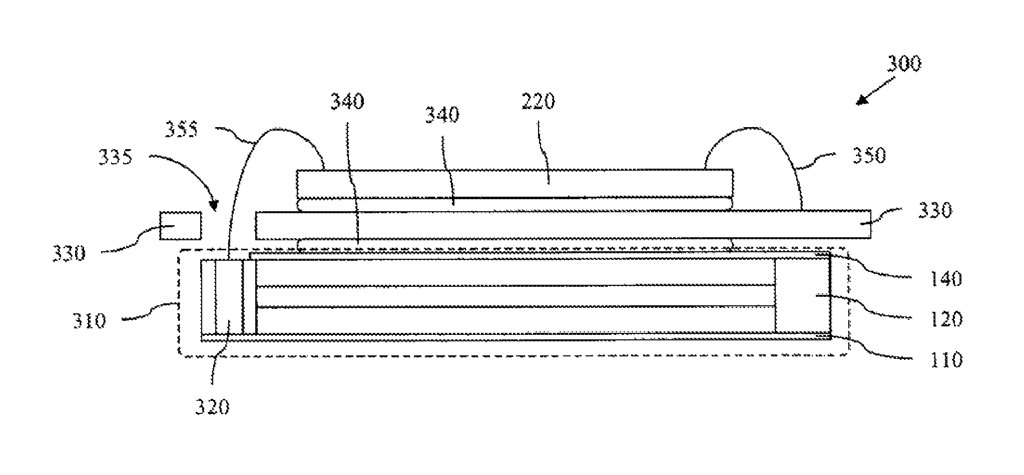
Referring to FIG. In FIG. 1A is shown a sectional diagram of at least a part of an embodiment of an apparatus in an intermediate manufacturing stage according to the aspects of this disclosure. The apparatus 100 comprises an electrode 110 coupled with a frame. The electrode 110 can be made of aluminum, copper or gold and/or any other electrically-conductive material. It may also be attached to the frame 120 using adhesives, bonding, brazing and clamps, as well as other mechanical fasteners. The thickness of the electrode 110 can range between 2 m and 20 m. Other thicknesses, however, are also included in the scope of this disclosure. In an exemplary embodiment at the nanoscale, for example, thickness can range from 10 nm to 100 nm.
The frame 120 comprises an opening 125 configured for receiving an energy device in accordance with aspects of the disclosure. The opening 125 can substantially or roughly correspond to the perimeter of an electronic device that will be coupled with and powered at least in part by the energy device. The perimeter of opening 125 can have a geometric shape that is substantially square, rectangular or circular or elliptical or any other regular or irregular shape with lateral dimensions between 7 nm to about 50 mm. In one implementation, the opening’s lateral dimension may be between 7 mm to 9 mm, while in another, it may be between 1 mm to 9 mm. In one implementation, opening 125 is substantially square with sides of approximately 1 mm.
The frame 120 can be formed by creating the opening 125 on a sheet or a plate of frame material. The frame material may consist of ceramics, plastics and/or electrically insulating substances. The frame material can be ceramic, fused silicon, or silicon carbide. However, other materials may also be included in the scope of this disclosure. The frame 120 can have a range of thicknesses between about 0.3mm and about 8mm. However, other thicknesses may also be within the scope. In an exemplary embodiment at the nanoscale, for example, the thickness could range from about 1 nm to about 20 nm. The opening 125 can be one of many openings that may be similar in the frame. These openings may be created by micromachining or laser machining or other methods such as casting, molding or stamping. The frame 120 can also include more than one material, such as electrically conductive or insulating materials. These multiple layers of materials may be joined vertically by adhesive, bonding and welding.
The electrode 110 can cover the entire frame 120 including the opening created by the opening 125. In another embodiment, however, the circumference of the electrode 110 could more closely match the perimeter 125 of the opening. The frame 120 can also include a shallow indentation or recess configured to receive electrode 110. The electrode 110 can be attached to the frame by pressing it into place or forming a friction or interference engagement between the edge of the electrode and the indentation of the frame.
Referring to FIG. In FIG. In FIG. 1A, an energy device 130 is formed or otherwise positioned within the opening 125. The following is an exemplary configuration for the energy stack 130, but other configurations are also included in the scope of this disclosure.
The energy device 130 may include more than two layers, and possibly more than one type of material. Separator layer 130b can be made of manganese or titanium, vanadium and/or any other material. In one implementation the separator 130 b is composed of lithium perchlorate, (LiClO4) combined with polyvinylidene. The separator 130 b can also, or alternatively, consist of a lithium salt that is cross-linked with polyethyleneoxide.
The electrode layers 130a and 130c are anode, cathode respectively of the energy device. The electrode layer may be either anode or cathode. The cathode can be made of disulfide or pentoxide in either case. The cathode can also be impregnated by p-type and n-type impurities and/or nanotechnology to improve cathode conductivity and charging performance. This may depend on the doping schemes used in the fabrication of microelectronic devices to be packaged together with the energy device.
The anode can be or include a metal-alloy film or foil which may be impregnated by lithium or lithium alloys impurities. Anodes may be impregnated by p-type and/or n-type impurities, or nano-technology elements to improve anode conductivity and charging performance. This could depend on the doping scheme used in the fabrication process of the microelectronic devices to be packaged together with the energy device. In one embodiment, in order to enhance the performance of the energy device 130, the anode can be impregnated with impurities that are opposite from the first type, such as n-type. The present disclosure does not limit itself to any specific doping scheme for the energy device or microelectronic devices to be packaged together with the device 130.
The energy device 130 may employ a lithium-manganese-dioxide chemistry, including those which are readily available commercially and/or otherwise understood by those skilled in the art. Another example of the energy device 130 chemistry may be lithium-titanium-disulfide (Li?TiSO2) or lithium-vanadium-pentoxide (Li?V2O5). As discussed above, impurities such as those used in semiconductor doping schemes can be added to the cathode or anode. The order of fabrication for the cathode 130 a, anode 130 b, and separator 130b within the frame may be determined by the fabrication process of the microelectronic devices to be packaged together with the energy device. The cathode, for example, may be associated (or fabricated simultaneously with) a n-type substrate or semiconductor layer. The anode can be associated in a similar way with a layer or substrate of p-type. The thickness of the energy device 130 can range between 200 m and 1000 m. However, other thicknesses may also be within the scope. The thickness of the device 130 can range from about 300 m to about 750m, for example. Each individual layer forming the energy devices layers 130 a – c can have a thickness between about 25 mm and 100 mm. In an example nano-scale implementation the thickness may range from about 1 nm to about 20 nm. For instance, where each of the individual layers of the energy devices 130 a-c are substantially less than 10 nm.
The anode can be made by cutting a rolled foil of lithium (possibly containing battery grade, 99.8% lithium) into 40-?m long ingots. The anode can also be alloyed, for example, with aluminum, manganese and/or copper.


Click here to view the patent on Google Patents.