Invented by Chung-Pin CHOU, Sheng-Wen Huang, Jun-Xiu Liu, Taiwan Semiconductor Manufacturing Co TSMC Ltd
Wafer defect inspection is a critical step in the semiconductor manufacturing process. It involves the identification and categorization of defects on the surface of silicon wafers, which are used as the base material for manufacturing integrated circuits. These defects can range from tiny particles and scratches to more complex issues like pattern deviations and electrical failures. Detecting and addressing these defects is essential to ensure the quality and reliability of the final semiconductor products.
Traditional methods of wafer defect inspection relied on manual visual inspection or rule-based algorithms. However, these methods were time-consuming, subjective, and prone to human errors. With the advent of machine learning, the semiconductor industry has witnessed a paradigm shift in defect inspection. Machine learning algorithms can analyze vast amounts of data and learn from it to identify patterns and anomalies, making them highly effective in detecting defects.
One of the key advantages of machine learning-based wafer defect inspection is its ability to handle complex and diverse defect patterns. Traditional methods often struggled to detect subtle defects or those with irregular shapes. Machine learning algorithms, on the other hand, can learn from a large dataset of labeled defects and develop a robust understanding of various defect types. This enables them to accurately classify defects and differentiate them from false positives, reducing the number of unnecessary rejections and improving overall yield.
Moreover, machine learning algorithms can adapt and improve over time. As they process more data and encounter new defect patterns, they can continuously update their models and enhance their accuracy. This adaptability is particularly beneficial in the semiconductor industry, where new defect types can emerge as manufacturing processes evolve.
The market for machine learning wafer defect inspection is expected to grow significantly in the coming years. According to a report by MarketsandMarkets, the global market size for wafer inspection systems is projected to reach $7.8 billion by 2026, with a compound annual growth rate of 12.1%. Machine learning-based solutions are expected to play a crucial role in driving this growth, thanks to their ability to improve inspection speed, accuracy, and efficiency.
Several key players in the semiconductor industry are already leveraging machine learning for wafer defect inspection. They are investing in research and development to develop advanced algorithms and systems that can handle the increasing complexity and miniaturization of semiconductor devices. These companies are also collaborating with research institutions and technology providers to enhance their machine learning capabilities and stay ahead in the market.
In conclusion, the market for machine learning wafer defect inspection is witnessing rapid growth due to the increasing demand for high-quality semiconductor devices. Machine learning algorithms offer superior accuracy, speed, and adaptability compared to traditional inspection methods. As the semiconductor industry continues to evolve, machine learning-based solutions will play a crucial role in ensuring defect-free and reliable semiconductor products.

The Taiwan Semiconductor Manufacturing Co TSMC Ltd invention works as follows
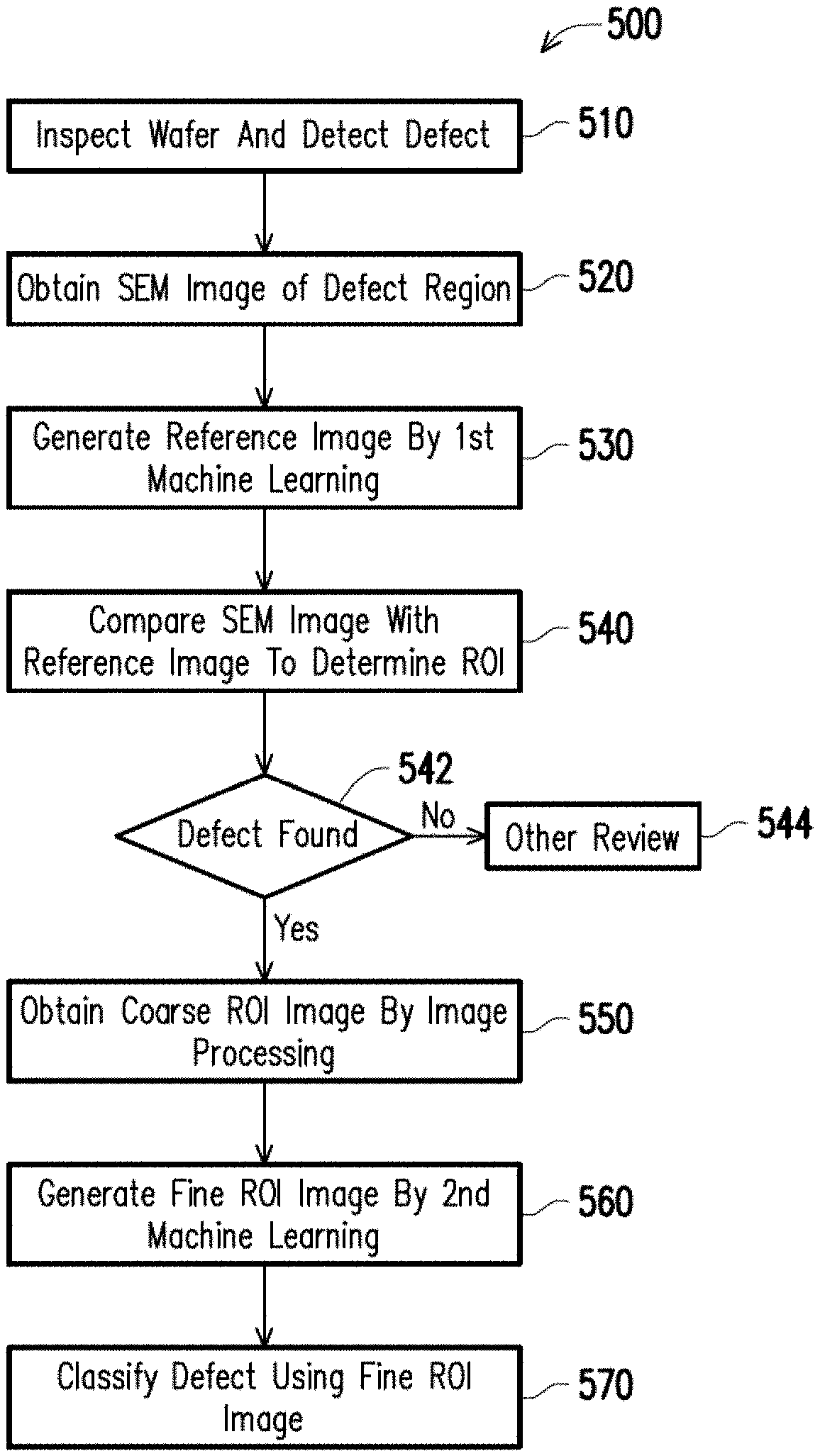
This disclosure is about solutions for detecting and classifying defects on wafers using machine learning. Machine learning techniques are used to classify and review defects on a wafer using only one digital microscope image with coarse resolution. The defect review and classification efficiency is improved because only one coarse SEM wafer image is required. The techniques are also not distracting and can be used in conjunction with other techniques for defect detection and classification.

Background for Machine learning wafer defect inspection
With the evolution of semiconductor technology, semiconductor dies become smaller and more features are integrated in a single die. These features are arranged in a tight pattern with minimal spacing between them. A semiconductor die is manufactured with more steps due to the higher feature density. Over a substrate, for example, complex exposure, development, and etching processes are performed. The wafer is checked for defects such as metrology offsets or shape deformations. If the inspection finds a defective wafer, it will then be reviewed by a defect review procedure, such as an automatic defect review. When a wafer is found to be defective, it will then undergo a defect review process. This may include an automatic defect review (?ADR?)
This disclosure is directed at solutions for detecting and classifying defects on wafers using machine learning techniques. The solutions use only a coarse resolution digital image of a wafer target, such as a scanning electronic microscope (?SEM?) Machine learning techniques are used to process the coarse SEM images to review and classify defects on the target wafer. The defect review and classification efficiency is improved because only one coarse SEM wafer image is required. The techniques are also not distracting and can be used in conjunction with other techniques for defect detection and classification.
Traditionally, a coarse SEM and a fine SEM are taken to classify or identify the defect on a wafer. In various embodiments, the disclosed techniques take only a single coarse SEM and analyze the coarse SEM to identify and classify the defect of the wafer. A wafer (referred to herein as a “target wafer”) is first inspected using a wide-range wafer inspection system. For example, the laser scanning pattern wafer defect inspection systems, in order to determine if a defect exists on the wafer. A defect region is identified on the wafer when the target wafer has been determined to be defective. The defect region is imaged using a digital microscope in coarse resolution. This is called a “coarse” image. Or a “first SEM” image. The term “SEM image” is used in the disclosure. As an example, the microscope image is described using this term. In one embodiment, the SEM image obtained is of a coarser resolution. This is enough to identify the defect but not to classify it or identify additional details for defect analysis. The coarse SEM images may have the same resolution as those used to identify defects in the conventional approach. The resolution of a SEM is relative and depends on the type of ICs or technology node formed on a wafer. “For example, a SEM image with a coarser resolution could be acceptable on an analog or mixed-signal IC but not acceptable on a digital IC due to the smaller structural dimensions of the digital IC.
In one embodiment, a first SEM is compared to a reference image in order to determine the defect(s) within the defect region. A (first) machine-learning process may be used to obtain the reference image through simulations. The simulation can be based on the wafer design, fabrication recipes or fabrication process parameters for the target wafer. A first machine-learning unit, for example, may use simulation or other techniques to translate wafer design information into a reference SEM image of the wafer surface. Machine learning techniques can be used, for example, to simulate the impact of fabrication processes on the geometry of features on a Wafer. The wafer design data feature geometries are then adjusted to reflect the simulation of fabrication process influences in order to produce the reference image. The reference image reflects how the fabrication process affects the shape of the structures of the wafer. In some embodiments, the image resembles an SEM image taken of a wafer that was made using the respective fabrication process. To improve simulation results or simulation processes (e.g. simulation algorithms), training and learning processes can be used. The simulated SEM of a wafer, for example, may be compared to an actual SEM, such as a “good” SEM. The comparison results may be used to update the simulation result and/or to update the simulation algorithms. The comparison results can be used to update simulation results and/or simulation algorithms. The reference image can be an SEM image from a wafer of the same design as the target, for example, a “good” wafer. The reference image may be a SEM image of a reference wafer that is comparable to the target wafer, e.g.,?good?
The first SEM of the target wafer will be compared to the reference image in order to locate the defect area or defect feature within defect region. The defect area or defect feature will usually be smaller and within the defect region. A defect feature or defect region is called a “region of interest” (?ROI?) in the following description. for descriptive purposes. A ROI image with a higher resolution, also known as a “fine ROI image”, is used to further examine the defect. for descriptive purposes.
The disclosed method does not take a second SEM image of the ROI. The fine ROI image (i.e. with higher resolution than the coarse SEM) is instead obtained through a secondary machine learning process. The ROI is extracted from a first SEM of the defect area using digital image processing techniques. The second coarse image is a portion of the original coarse image. The image resolution won’t improve by extracting the second SEM image from the original image. It will either stay the same, or become coarser. The second SEM is therefore a coarse image. The second machine-learning unit maps the second image of the ROI using a database with image feature details of higher resolution. Each image feature detail can be saved as a smaller image with a finer resolution that can be substituted for a portion of the second coarse picture. Each piece of image feature detail can be referred to by the term “image patch” for descriptive purposes. The image patch is higher resolution and contains more details than a part of the second coarse images. If a match can be made between a portion of the second fine image and the image patch, then the image patch will replace the part of second coarse image. The image patch replaces all of the portions of the second coarse images. This results in a finer-resolution image. In one embodiment, mapping can be performed based on identification elements included in the second coarse images, also referred to by the term “feature identifier”. The second SEM coarse images can be divided into parts, and then the feature identifiers assigned to each part. The feature identifiers can be used to map image patches within the database. Mapped image patches can be used to complement or replace the partition parts. The ROI fine image is created when all partition parts are replaced by the image patches. In one embodiment, the mapping of partition parts to image patches and the partitioning of the second coarse images may be repeated multiple times in order to produce a fine ROI image. The second coarse image can be divided differently in order to create different partition parts that are mapped with the image patches. In one embodiment, the image patches mapped to the coarse image can be used to refine its partitioning. If, for example, two image patch details on two adjacent partitions of the second coarse images are inconsistent, e.g. the features of the two patches do not match up, the ROI can be re-partitioned in order to avoid this problem.
In one embodiment, rules may be applied to the selection or filtering of the image patches in order to produce a list of image patch to be used to generate the fine ROI image. The rules could, for example, require that the surface features of a partition portion immediately adjacent to the second coarse ROI image be consistent. The rules can also specify that surface features in the fine images must be consistent with design data on the target wafer.
In one embodiment, the second machine-learning unit’s feature map may contain multiple levels of image patches that correspond to different levels of partition parts. The feature identifier from the ROI’s second coarse image may be mapped to the first tier image patches in the feature map. The first tier may include image patches with a scale of resolution that is higher than the second coarse image. The first tier image patches mapped may be further divided to obtain a secondary tier feature identifiers. The second tier features identifiers can be mapped to a second layer of image patches with a finer scale of resolution than the first. Rules may be used to limit the mapping in one or more mappings. The rules could, for example, stipulate that the proposed features details of adjacent partitions must be consistent in each tier. The rules can also specify that in each level of mapping the feature details mapped must be consistent with design data for the target wafer.
An existing image patch can be selected. A patch can also be created based on nearby feature details. Further, the generation or selection of an image patch for a particular partition part can be trained along with the generation or selection of image patches adjacent to that partition part. The disclosure allows for a variety of training methods. The disclosure does not limit itself to any particular training approach in the selection or creation of image patches.
The ROI fine resolution image is created after the image patches have been selected to a scale or tier of image resolution. The ROI fine resolution image is used to classify defects on the wafer target to determine a defect type, cause or any other detailed analysis. The fine image of ROI can be partitioned further into partition parts which are then mapped using image patches with a finer resolution.

The feature maps of the second unit machine learning may be updated by new data based on the SEM images with fine resolution available to the second unit machine learning. After a machine learning process generates a fine-resolution image of an ROI, capturing a fine-resolution image of the ROI can be done. The fine resolution image can be divided into patches and linked to feature identifiers in the second coarse image. The generated fine-resolution image can be compared with the actual SEM fine-resolution image to determine if the generated image matches the fine-resolution SEM. The results of the comparison can be used to calibrate the machine-learning algorithm for partitioning coarse images, or mapping partition parts onto image patches. The second machine learning unit can compare an image patch with the partition portion of the fine resolution image in order to determine if the image patch matches the fine resolution image. If the selected patch does not match the fine resolution image in question, the algorithm for selecting/generating image patches or the stored images patches can be updated to ensure that the correct patch is selected/generated.
FIG. FIG. 1 shows an example wafer defect control system 100. FIG. As shown in FIG. The wafer manufacturing system 110 is configured for processing a wafer in order to form integrated circuits. The wafer manufacturing on-site system includes multiple stages 112. These stages process a single wafer sequentially. A wafer is typically prepared in a semiconductor manufacturing process. This can be a whole wafer with a diameter of 8, 12, 16 or other sizes. The wafer is then used to form circuitry. Circuitry is formed on the wafer. ), middle-of-line, (?MOL? The FEOL processes include wafer preparation, isolation, well formation and gate patterning. The FEOL process includes wafer preparation and isolation, gate patterning and implantation of spacers, extensions, source/drain implantation and silicide, as well as dual stress liner and source/drain implantation. MOL includes gate and/or drain contact formation. BEOL includes all wafer fabrication steps that follow the MOL and FEOL. For example, forming wirings to interconnect individual devices in metallization layer. The dielectric layers that separate the metallization layers (inter-layer dielectric, or ILD) are used to interconnect individual devices. layers. ILD layers can be made of silicon oxide or dielectrics with low-k. The circuitry is then sawn off the wafer after it has been formed. The dice are tested and packaged in order to produce individual integrated circuit products. The wafer fabrication system on-site 110 includes all toolsets required for processing the wafer as a whole or sawn, such as a die.
The wafer inspection system 120 may be an integrated part of the wafer fabrication on-site system 110 or may be configured to function together with the wafer fabrication on-site system 110 as a standalone device. The wafer inspection system 120 may include one or more laser-based inspection devices, ultrasonic inspection devices, transducers, electron beam based inspection devices, bright-field inspection devices, dark-field inspection devices, other metrology devices, and/or other devices suitable for wafer defect inspections. For example, the wafer inspection system 120 may include one or more of beam guns, photomultiplier tubes, E-beam tilts, silicon drift detectors, optical microscopes, microscope beam controllers, attenuation and scan amplifiers, or internal transfer units. The wafer inspection system 120 may be configured to inspect wafers in various stages 112 of fabrication, e.g., patterned wafers, whole wafers, sawn wafers, JEDEC trays, multi-chip modules, or other stages of wafer processing. The wafer inspection system 120 may use a same or a different inspection device for inspecting a wafer at different stages 112 of the wafer fabrication system 110.
The wafer inspection system is configured to inspect wafers for defects at any stage in the semiconductor manufacturing process. The defect may include any defects, e.g., metallization defect, diffusion defect, passivation layer defect, scribing defect, glassivation defect, or interconnect defects. Defects may also be a deviation or variation in dimension according to the wafer fabrication process. These defects can be random or systematic. A defect can be visible or not visible on the surface of a silicon wafer. “For example, the patterned wafer inspecting device detects defects by comparing adjacent die images, which will be sawn apart into individual dies. It then calculates the difference between adjacent die images.
If the wafer-inspection system 120 determines a wafer contains a defect, it is then presented to the defect review 130 system as a target for further analysis. A defect region is defined on the target wafer as the region surrounding and/or covering the probable defect. Normaly, the wafer inspection system 120 is a submicron inspection between 0.1 micron and about 1 micron. The defect area is usually a small circle with a diameter between 1 micron and 10 microns or larger.
The defect review 130 system may include an imaging unit such as a scanner electron microscope (?SEM?) One or more machine-learning units are also described herein. The defect review system is configured to identify defects or defect areas, also known as a “region of interest” (?ROI?) The wafer inspection system has identified a defect in the region of the target waver. The defect review system is configured to also obtain a coarse SEM image of the wafer target, which can be referred to by the term “first SEM image.” The defect review system 130 is also configured to obtain a coarse image (also referred to as “first SEM image”) of the target wafer, or to generate a second coarse image (also referred to a “second coarse image”) of the ROI. To generate a fine ROI image. The fine image is sent to defect classification system 140.
The defect classification system is designed to identify one or more characteristics or causes of defects, such as a type, size, circuitry location, function element or other characteristics, at least in part, using the outputs from the defect review system, for example, the fine image ROI.
FIG. FIG. 2 shows an example of a defect review system 130. Referring to FIG. The defect review system 130 consists of one or more imaging units 210, an ROI determination unit 220, coarse ROI image unit (240) and fine ROI image unit (250). The reference image unit 220-, the ROI-determination unit 230-, the coarse ROI-image unit 240 or the fine ROI-image unit 250 can be implemented by a computing device such as a server computer. The elements of the system 130 can reside on a single computing device (e.g. a server computer) or in separate devices connected via a network to each other in a distributed computing setting, such as a cloud computing environment. In different embodiments, the defect review system may consist of one or more components that reside on the same computing device. They can communicate with each other via network communications. The ROI determination unit and the coarse ROI images unit may, for example, reside on the same computing device. Other variants on the physical arrangements/configurations of the system 130 components are also possible, which are all within the scope of the disclosure.
In operation the imaging unit is configured to acquire a first picture of a wafer target. The first image is, for example, a SEM. The first SEM of the wafer can be a two-dimensional or three-dimensional picture of the wafer’s surface. In one embodiment, the SEM image can cover the entire surface of the wafer. In a second embodiment, the SEM image is only a part of a surface, called ‘first portion? The first portion covers a portion, referred to as?first part? of a target wafer’s surface. The first portion surrounds the defect area identified by the wafer-inspection system 120. The first SEM has a resolution which is relatively coarse compared to an image resolution requirement for the defect classification system or a finer-resolution image of a ROI, as described in this document. The ‘coarseness’ of the first SEM image should be understood. The ‘coarse’ resolution of the SEM image 1 is only defined in relation to the finer image resolution. Resolution does not convey an absolute standard or criterion regarding the resolution for the first SEM. “In an embodiment, the first coarse SEM image is a resolution that ranges from about 1.4nm to 0.1micron.
FIG. “FIG. 3A shows an example of a coarse first SEM image for a portion 300 of a target wafer. The first portion contains a defect area 310 and non-defect parts 320. A sample image resolution for the FIG. “The image resolution of the FIG. 3A is approximately 2.5 nm/pixel.

The first coarse SEM is stored, in one embodiment, in a inspected image database that is coupled to the imaging device 210. The inspected image databases also store other inspected images in different image resolutions of other wafers.
![]()
Click here to view the patent on Google Patents.