Invented by Kazemi varnamkhasti; Hamidreza, Jin; Zhang, Ismail; Aly, Cappabianca; David P.


Inductors have always been a key part of radio frequency (RF) chips. They help store energy, filter signals, and keep our devices running smoothly. But making them smaller and better is a huge challenge. A recent patent application introduces a new way to build inductors using magnetic films and special patterns called trenches. In this article, we’ll walk through the background, the science, and the invention itself, making it all easy to understand.
Background and Market Context
If you have used a phone, a wireless speaker, or a smart gadget, you have already relied on tiny parts called inductors. These sit deep inside the chips that power modern electronics. Inductors help filter out noise, tune signals, and make wireless communication possible. Without them, your calls would drop and your music would sound fuzzy.
Over the years, new mobile networks like 5G have pushed chip makers to pack more power into smaller spaces. Everyone wants their devices to be faster, thinner, and more reliable. This means each part, including the humble inductor, must be made smaller without losing its performance.
But shrinking inductors is not easy. When you make them smaller, they store less energy and become less efficient. Chip designers have to find smart ways to squeeze more performance into less space. If they can do this, they can make phones last longer on a single charge, improve call quality, and enable new technologies like the Internet of Things.
Companies everywhere are racing to solve these problems. There is big money at stake. Every improvement can mean better products and happier customers. So, inventors are always looking for new materials and designs that can give their chips an edge.

Recently, using magnetic films around inductors has become a promising approach. Magnetic films can help boost the inductor’s ability to store energy, but they also come with problems, like causing unwanted losses. The patent we’ll explore today offers a clever way to get all the benefits of magnetic films while avoiding their downsides. This could be a game changer for the electronics industry.
Scientific Rationale and Prior Art
To see why this invention is important, let’s first understand how a basic inductor works and what challenges engineers face.
An inductor is a simple piece of wire shaped in a loop or coil. When current flows through the wire, it creates a magnetic field. This field stores energy. The bigger the field, the more energy the inductor can hold. In RF chips, these inductors are made using tiny traces of metal, often copper, placed on top of a silicon chip.
One of the main ways to judge how good an inductor is involves something called the “Q factor,” or quality factor. This is a measure of how well the inductor stores energy compared to how much energy it loses. A higher Q factor means a better inductor.
But there’s a problem. As you make the inductor smaller, it stores less energy. To make up for this, engineers started wrapping the metal trace with thin layers of magnetic material, called magnetic films. These films boost the magnetic field, letting the inductor store more energy in less space.
Sadly, there’s no free lunch. Magnetic films have a downside: they make it easier for unwanted currents, called eddy currents, to form. Eddy currents act like tiny thieves, stealing energy and lowering the Q factor. If the films are too thick, these losses become even worse. This means you can’t just add more magnetic film and expect things to get better.


Over the years, many have tried to solve this problem. Some used very thin magnetic films, hoping to keep the eddy currents small. Others patterned the films into stripes or patches, trying to break up the path for these unwanted currents. A few tried sandwiching magnetic films with insulating layers, called dielectrics, to make it harder for eddy currents to flow.
But these solutions always involved trade-offs. Making the films too thin or too broken up lowers the boost they give to the magnetic field. Using more layers adds cost and complexity. No one has found a design that gives a strong magnetic field and a high Q factor, without making the inductor too big or too expensive.
This is the challenge the new invention sets out to solve. The inventors realized they could carefully pattern the magnetic films around the inductor using special trenches, or gaps, filled with an insulator. By placing these trenches in just the right spots, they can stop the eddy currents without losing too much magnetic field strength. Even better, by stacking several layers of magnetic film and aligning the trenches across the top, bottom, and sides, they can build a dense, 3D shield around the inductor. This approach keeps the inductor small, boosts the Q factor, and avoids the usual losses.
In short, the patent offers a smart way to get the best of both worlds: small inductors with strong fields and low losses, ready for the next generation of wireless technology.
Invention Description and Key Innovations
Now, let’s look closely at what the patent actually claims and how this new inductor is built and works.

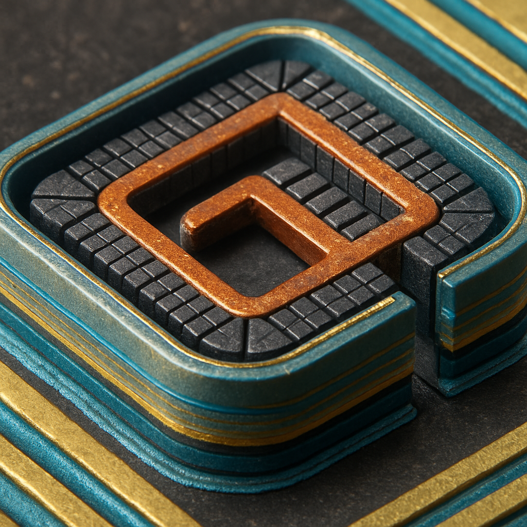
At the heart of the invention is a familiar part: a conductive trace, which is just a small wire made of metal like copper. This trace is shaped into a loop or coil to form the inductor. The magic happens in what wraps around this trace.
The inventors surround the conductive trace with one or more layers of magnetic film. These films are not just simple coatings. They are carefully divided into sections using trenches, which are thin gaps filled with an insulator like air or a plastic called polyimide.
Here’s the clever part: the trenches are placed along the length and width of the inductor, both above and below the metal trace. This cuts the magnetic film into small islands or patches. Because the patches are separated by the trenches, eddy currents can’t easily flow from one patch to another. This sharply reduces the energy lost to these unwanted currents.
Even more, the trenches can be lined up above and below the trace, and even across its thickness, creating a 3D pattern of separated magnetic islands. By stacking several layers of these patterned films, with each layer separated by a thin dielectric, you get a powerful magnetic shield with very little loss. The distance between each layer, and between the layers and the metal trace, can be tuned to get the best performance.
The patent covers many ways to build this structure. The trace and films can be made directly on top of the silicon chip (in what’s called the BEOL structure), in a redistribution layer (RDL) on the chip, or even as a separate chiplet (called an integrated passive device, or IPD) that’s attached to the main chip. The multi-layer stacks can be made using standard processes like lamination, etching, and deposition, making them practical for high-volume chip production.
The real breakthrough is in the careful placement and patterning of the trenches. The inventors show that by aligning the trenches in multiple directions, you can control the size and shape of the magnetic patches, optimizing the balance between boosting the magnetic field and cutting down losses. The size of each patch, the width of each trench, and the number of layers can all be adjusted to match the needs of different chips and frequencies.
Tests described in the patent show that this design can shrink the size of the inductor while keeping its performance high. For example, by using three layers of magnetic film, each cut into small patches by a grid of trenches, you can build an inductor that fits in a much smaller space yet has a higher Q factor than older designs. By adding more layers while making each one thinner, you can push the Q factor even higher.
The invention also makes it possible to use the same basic design for many different types of chips and packages. Whether you need a single-turn inductor, a multi-turn coil, or a custom shape for a special application, the same approach works. You can wrap the multi-layer magnetic stack around just the top and bottom, or all the way around the sides, or even at angles, depending on what the circuit needs.
By using regular chip-making steps like etching and lamination, the invention can fit into current chip factories without special tools or materials. This means it is not just a lab trick—it can be used in real products, right away.
In the end, this new way of making tiny inductors—by wrapping them with carefully patterned magnetic films and dividing the films into small islands using smart trench patterns—opens the door to faster, smaller, and more efficient RF chips. It could help make the next generation of phones, wearables, and smart devices even better than before.
Conclusion
Inductors are quiet heroes inside every wireless device. Making them better has always been a tough job, especially as our gadgets get smaller and more powerful. This new patent brings a fresh idea: surround the inductor with layers of magnetic film, but break up the film with special trenches that block energy losses. By stacking these patterned films in three dimensions and adjusting their size, shape, and position, designers can build tiny inductors that keep up with the demands of modern technology.
This invention is not just about clever engineering. It is about helping everyone enjoy better performance from the devices they use every day. With this approach, chip makers can pack more into less space, save energy, and make new features possible. As wireless technology keeps moving forward, smart innovations like this will be the key to what comes next.
Click here https://ppubs.uspto.gov/pubwebapp/ and search 20250218637.